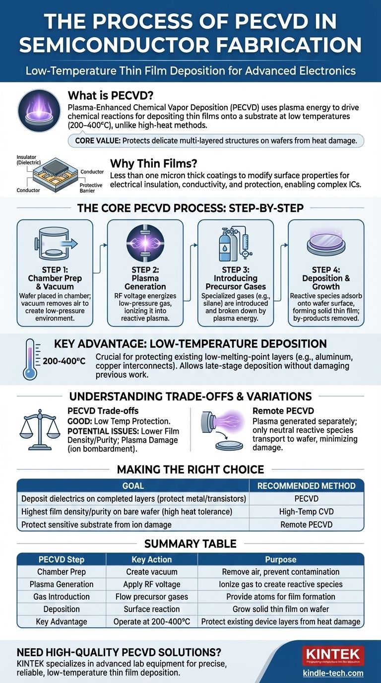
In semiconductor fabrication, Plasma-Enhanced Chemical Vapor Deposition (PECVD) is a process used to deposit thin films of material onto a substrate, such as a silicon wafer. Unlike conventional methods that require high heat, PECVD uses energy from a plasma to drive the chemical reactions, allowing for high-quality film deposition at significantly lower temperatures.
The core value of PECVD lies in its ability to deposit essential insulating or conductive films at low temperatures. This protects the delicate, multi-layered structures already built on a semiconductor wafer, which would be damaged or destroyed by high-heat processes.
Why Thin Films Are Critical in Semiconductors
Modifying Surface Properties
Thin films are coatings, often less than one micron thick, that are applied to a substrate to fundamentally change its surface properties. This is a foundational technique in modern electronics manufacturing.
Essential Roles in a Chip
In a semiconductor device, these films serve critical functions. They can act as electrical insulators (dielectrics), conductors, or protective barriers against corrosion and wear, enabling the creation of complex integrated circuits.
The Core PECVD Process: A Step-by-Step Breakdown
Step 1: Chamber Preparation and Vacuum
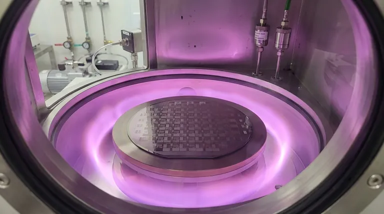
The substrate (wafer) is placed inside a reaction chamber. A vacuum system removes the air, creating a low-pressure environment necessary to sustain a plasma and prevent contamination.
Step 2: Plasma Generation
An external energy source, typically radio-frequency (RF) voltage, is applied to an electrode within the chamber. This energizes the low-pressure gas, causing it to ionize and form a plasma, often seen as a characteristic glow discharge.
Step 3: Introducing Precursor Gases
Specialized precursor gases, which contain the atoms needed for the desired film (e.g., silane for silicon films), are introduced into the chamber. The high energy of the plasma breaks these gas molecules apart into highly reactive chemical species (ions and radicals).
Step 4: Deposition and Film Growth
These reactive species diffuse through the chamber and adsorb onto the cooler surface of the wafer. They then react on the surface, forming a solid, stable thin film. Unwanted by-products from the reaction are continuously removed by the vacuum pump.
The Key Advantage: Low-Temperature Deposition
Protecting Existing Structures
The defining feature of PECVD is its low operating temperature, often in the range of 200-400°C. A modern microprocessor has many layers, including metal interconnects (like aluminum or copper) that have low melting points.
Enabling Complex Devices
High-temperature deposition methods (often >600°C) would melt or damage these previously fabricated layers. PECVD allows for the deposition of critical films late in the manufacturing process without destroying the work already done, making it indispensable for advanced electronics.
Understanding the Trade-offs
Film Quality vs. Temperature
While good, PECVD films can sometimes have a lower density or contain more impurities (like hydrogen from precursor gases) than films deposited using high-temperature methods. The lower thermal energy means atoms may not arrange themselves into a perfectly ordered structure.
Potential for Plasma Damage
The high-energy ions within the plasma can bombard the wafer surface during deposition. This physical impact can sometimes introduce defects or stress into the substrate or the film itself.
An Important Variation: Remote PECVD
To mitigate plasma damage, a technique called Remote PECVD is used. In this method, the plasma is generated in a separate area, and only the chemically reactive, but electrically neutral, species are transported to the wafer. This protects the sensitive substrate from direct ion bombardment.
Making the Right Choice for Your Goal
When selecting a deposition method, the decision is always driven by the specific requirements of the manufacturing step.
- If your primary focus is depositing dielectric films on completed device layers: PECVD is the default choice to avoid thermal damage to existing metal interconnects and sensitive transistors.
- If your primary focus is achieving the highest possible film density and purity on a bare wafer: High-temperature Chemical Vapor Deposition (CVD) may be superior, but only if the substrate can tolerate extreme heat.
- If your primary focus is protecting a highly sensitive substrate from any ion damage: Remote PECVD provides the benefits of low temperature while minimizing the risk of plasma-induced defects.
Ultimately, PECVD is a cornerstone technology that enables the complexity and density of modern semiconductor devices by solving the critical challenge of low-temperature film deposition.
Summary Table:
| PECVD Step | Key Action | Purpose |
|---|---|---|
| Chamber Prep | Create vacuum | Remove air, prevent contamination |
| Plasma Generation | Apply RF voltage | Ionize gas to create reactive species |
| Gas Introduction | Flow precursor gases | Provide atoms for film formation |
| Deposition | Surface reaction | Grow solid thin film on wafer |
| Key Advantage | Operate at 200-400°C | Protect existing device layers from heat damage |
Need high-quality PECVD solutions for your semiconductor fabrication? KINTEK specializes in advanced lab equipment and consumables for precise thin film deposition. Our expertise ensures reliable, low-temperature processes that protect your delicate wafer structures. Contact our experts today to discuss how our PECVD systems can enhance your semiconductor manufacturing yield and performance.
Visual Guide
Related Products
- RF PECVD System Radio Frequency Plasma-Enhanced Chemical Vapor Deposition RF PECVD
- Inclined Rotary Plasma Enhanced Chemical Vapor Deposition PECVD Equipment Tube Furnace Machine
- Chemical Vapor Deposition CVD Equipment System Chamber Slide PECVD Tube Furnace with Liquid Gasifier PECVD Machine
- Inclined Rotary Plasma Enhanced Chemical Vapor Deposition PECVD Equipment Tube Furnace Machine
- Microwave Plasma Chemical Vapor Deposition MPCVD Machine System Reactor for Lab and Diamond Growth
People Also Ask
- How does plasma enhance CVD? Unlock Low-Temperature, High-Quality Film Deposition
- What is the role of RF-PECVD in VFG preparation? Mastering Vertical Growth and Surface Functionality
- What is an example of PECVD? RF-PECVD for High-Quality Thin Film Deposition
- Why is a Matching Network Indispensable in RF-PECVD for Siloxane Films? Ensure Stable Plasma and Uniform Deposition
- What is plasma chemical vapor deposition? A Low-Temperature Thin Film Coating Solution