At its core, semiconductor thin film manufacturing is the process of depositing exceptionally thin, precisely controlled layers of various materials onto a substrate, typically a silicon wafer. This is accomplished through two primary methods: Chemical Vapor Deposition (CVD), which uses chemical reactions to build layers, and Physical Vapor Deposition (PVD), which physically transfers material onto the wafer. The choice between these methods is dictated by the specific material being deposited and its intended electrical function within the final microchip.
The goal of thin film deposition is not merely to coat a surface. It is the atomic-scale construction process used to build the fundamental components of an integrated circuit—the transistors, insulators, and wires—one layer at a time.
The Foundation: Why Thin Films Are Essential
To understand the manufacturing process, you must first understand the purpose of the films themselves. A modern microchip is a three-dimensional structure built from hundreds of these layers.
From Substrate to Circuit
The process begins with a pristine, flat substrate, most often a wafer of crystalline silicon.
Each thin film layer adds a new material with a specific electrical property, gradually building the complex architecture of an integrated circuit.
The Role of Each Layer
These layers are not interchangeable. They fall into three main categories that work together to form active components like transistors.
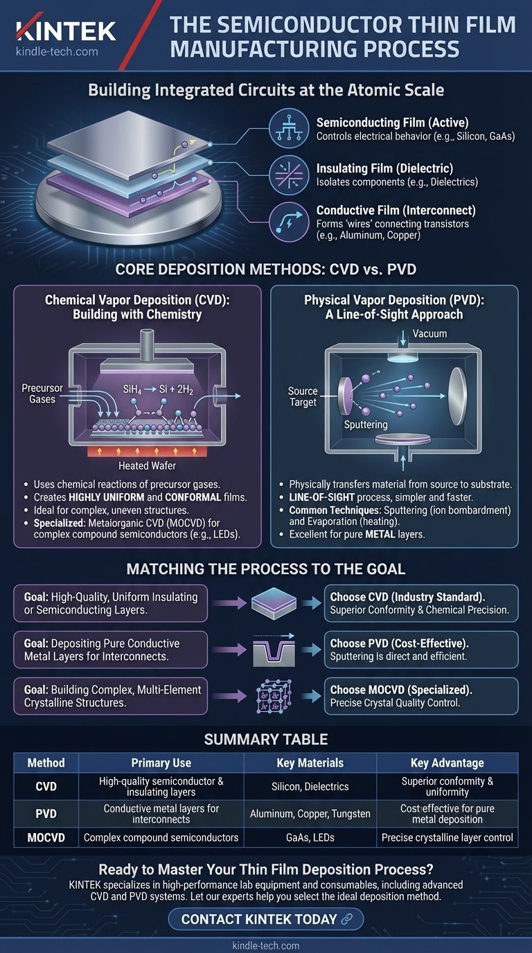
- Semiconducting Films: These are the active layers where electrical behavior is controlled, often made of silicon (Si) or more complex compound semiconductors like gallium arsenide (GaAs).
- Insulating Films (Dielectrics): These films prevent electricity from flowing where it shouldn't. They isolate different conductive parts from each other.
- Conductive Films: These form the "wires" or interconnects that link the millions or billions of transistors on a chip. Materials include metals like aluminum, copper, and tungsten.
Core Deposition Methods: CVD vs. PVD
The vast majority of thin film manufacturing falls into two families of techniques. The method chosen is critical to the quality and function of the layer being built.
Chemical Vapor Deposition (CVD): Building with Chemistry
CVD is the dominant process for creating the highest-quality semiconductor and dielectric films due to its precision.
The process involves introducing precursor gases into a reactor chamber containing the wafers. These gases react on the hot wafer surface, leaving behind a solid film of the desired material. For example, silane gas (SiH4) is used to deposit a solid film of pure silicon (Si).
This method excels at creating highly uniform and conformal films, meaning the layer's thickness is consistent even over the complex, uneven topography of a partially built chip.
A Deeper Look: Metalorganic CVD (MOCVD)
For complex semiconductors made of multiple elements (like GaAs), a specialized variant called MOCVD is used.
This advanced process uses metalorganic compounds as precursors to grow perfect crystalline layers, enabling the creation of high-performance devices like LEDs and advanced transistors.
Physical Vapor Deposition (PVD): A Line-of-Sight Approach
PVD works by physically moving material from a source (or "target") to the substrate, much like spray painting, but on an atomic level.
This is a "line-of-sight" process, meaning the deposited atoms travel in a straight line from the source to the wafer. It is simpler and often faster than CVD.
Common PVD Techniques
The two most common PVD methods are sputtering, where the target material is bombarded with ions to eject atoms, and evaporation, where the target is heated until it vaporizes. These methods are excellent for depositing very pure layers of metals.
Understanding the Trade-offs
Neither method is universally superior; they are tools selected for a specific job. The choice is a classic engineering trade-off between performance, material properties, and complexity.
When to Use CVD
CVD is the default choice when conformity and film quality are non-negotiable.
It is essential for depositing the critical insulating layers that isolate components and the high-purity semiconductor layers that form the transistors themselves. Its ability to uniformly coat intricate structures is its defining advantage.
When to Use PVD
PVD is primarily used for depositing conductive metal layers.
Because its role is often to fill wider trenches to form wires, the "line-of-sight" limitation is less of a concern. It is a reliable and cost-effective method for creating the chip's interconnect wiring, such as layers of aluminum, copper, or barrier metals like titanium nitride (TiN).
The Final Step: Patterning the Film
Deposition alone does not create a circuit. After a film is uniformly deposited across the entire wafer, photolithography and etching are used to remove material, leaving behind the precise patterns that define the final circuit components.
Matching the Process to the Goal
To make the right choice, you must align the deposition technique with the function of the layer you are creating.
- If your primary focus is creating high-quality, uniform insulating or semiconducting layers: CVD is the industry standard due to its superior conformity and chemical precision.
- If your primary focus is depositing pure conductive metal layers for interconnects: PVD techniques like sputtering are the most direct and cost-effective solution.
- If your primary focus is building complex, multi-element crystalline structures for advanced devices: A specialized process like MOCVD is required for its precise control over the material's crystal quality.
Ultimately, mastering these atomic-scale deposition methods is what enables the relentless miniaturization and increasing power of all modern electronics.
Summary Table:
| Method | Primary Use | Key Materials | Key Advantage |
|---|---|---|---|
| Chemical Vapor Deposition (CVD) | High-quality semiconductor & insulating layers | Silicon, Dielectrics | Superior conformity & uniformity |
| Physical Vapor Deposition (PVD) | Conductive metal layers for interconnects | Aluminum, Copper, Tungsten | Cost-effective for pure metal deposition |
| Metalorganic CVD (MOCVD) | Complex compound semiconductors | GaAs, LEDs | Precise crystalline layer control |
Ready to Master Your Thin Film Deposition Process?
Whether you are developing next-generation transistors or optimizing your chip interconnects, the right deposition equipment is critical. KINTEK specializes in providing high-performance lab equipment and consumables for semiconductor manufacturing, including advanced CVD and PVD systems.
Our solutions help you achieve the precise, uniform layers required for cutting-edge microchips. Let our experts help you select the ideal deposition method for your specific materials and application goals.
Contact KINTEK today to discuss how our specialized lab equipment can enhance your semiconductor research and production capabilities.
Visual Guide
Related Products
- Aluminized Ceramic Evaporation Boat for Thin Film Deposition
- Tungsten Evaporation Boat for Thin Film Deposition
- Electron Beam Evaporation Coating Oxygen-Free Copper Crucible and Evaporation Boat
- Molybdenum Tungsten Tantalum Evaporation Boat for High Temperature Applications
- HFCVD Machine System Equipment for Drawing Die Nano-Diamond Coating
People Also Ask
- What is the widely used boat made of in thermal evaporation? Choosing the Right Material for High-Purity Deposition
- Why is an alumina boat and Ti3AlC2 powder bed necessary for Ti2AlC sintering? Protect MAX Phase Purity
- What are the alternatives to sputtering? Choose the Right Thin Film Deposition Method
- Why are high-purity ceramic boats used for lignin activation? Ensure Purity & Thermal Stability
- What is the source of evaporation for thin film? Choosing Between Thermal and E-Beam Methods


