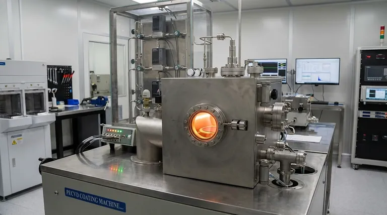
The process of silicon nitride Plasma-Enhanced Chemical Vapor Deposition (PECVD) is a method for depositing a thin film onto a substrate by using an energized plasma to drive a chemical reaction between precursor gases. In a vacuum chamber, a silicon source gas (like silane) and a nitrogen source gas (like ammonia) are introduced. Radio frequency (RF) energy is then applied, creating a plasma that breaks down the gases into reactive species, which then react and deposit on the substrate as a solid silicon nitride film at relatively low temperatures.
At its core, PECVD substitutes the intense heat required by traditional methods with the energy of a plasma. This allows for the creation of high-quality, dense silicon nitride films at temperatures low enough to be safe for sensitive electronic components, making it a cornerstone of modern semiconductor manufacturing.
How PECVD Works: A Step-by-Step Breakdown
The PECVD process for silicon nitride is a carefully controlled sequence designed to build a uniform, high-quality film layer by layer.
Introducing the Precursors
The process begins by introducing volatile precursor gases into a vacuum chamber containing the substrate (e.g., a silicon wafer). The primary precursors are a silicon source, typically silane (SiH₄), and a nitrogen source, most commonly ammonia (NH₃).
Generating the Plasma
Once the gases are stabilized, radio frequency (RF) or microwave energy is applied to the chamber. This energy ionizes the gas molecules, stripping electrons and creating a low-temperature plasma—a highly reactive cloud of ions, radicals, and other excited species.
The Chemical Reaction
The high energy of the plasma, rather than high heat, facilitates the chemical reaction. The reactive species from the precursor gases combine to form silicon nitride, as summarized by the general reaction: SiHₓ + NH₃ → SiₓNᵧH₂ + H₂.
Film Deposition and Growth
The newly formed silicon nitride molecules deposit onto the relatively cool surface of the substrate. This process continues, building up a solid, thin film of silicon nitride with a uniform thickness across the entire surface.
The Core Advantage: Plasma Over Heat
The defining feature of PECVD is its ability to perform deposition at significantly lower temperatures than conventional thermal Chemical Vapor Deposition (CVD).
Lower Deposition Temperatures
Traditional thermal CVD requires temperatures of 700°C or higher to provide the energy needed for the chemical reaction. PECVD achieves this at much lower temperatures, often in the range of 200-400°C, because the plasma provides the necessary reaction energy.
Protecting Underlying Components
This low-temperature process is critical in semiconductor fabrication. It allows silicon nitride to be deposited on a wafer without damaging or altering previously fabricated structures, such as the delicate metal interconnects that would be destroyed by high temperatures.
High-Quality Film Properties
Despite the lower temperature, PECVD produces films with excellent characteristics. They are known for being dense, highly insulating, and acting as a superior barrier against contaminants like sodium ions (Na⁺), which can degrade device performance.
Understanding the Trade-offs and Considerations
While powerful, the PECVD process has nuances that engineers must manage to achieve the desired results.
The Role of Hydrogen
The chemical equation for the process reveals that the resulting film is actually a hydrogenated silicon nitride (SiₓNᵧH₂). This incorporated hydrogen is a direct result of the low-temperature process and can significantly influence the film's electrical properties and mechanical stress.
Critical Process Control
The final properties of the silicon nitride film—such as its density, dielectric constant, and stress—are not fixed. They depend heavily on a precise balance of process parameters, including gas flow rates, chamber pressure, RF power, and temperature.
Managing Film Stress
PECVD films inherently possess internal mechanical stress (either compressive or tensile). This stress must be carefully controlled, as high levels can cause the film to crack, peel away from the substrate, or even warp the entire wafer.
How to Apply This to Your Project
Choosing the right deposition method depends entirely on the constraints and goals of your application.
- If your primary focus is compatibility with integrated circuits: PECVD is the standard choice for depositing silicon nitride as a passivation or dielectric layer on devices with existing metal structures.
- If your primary focus is achieving the highest purity film: A high-temperature thermal process like LPCVD (Low-Pressure CVD) will yield a film with less hydrogen, but it cannot be used on temperature-sensitive substrates.
- If your primary focus is tuning specific film properties: PECVD offers the flexibility to adjust the film's refractive index, stress, and etch rate by carefully modifying the recipe parameters.
Ultimately, PECVD masters the critical manufacturing challenge of creating a robust, high-performance protective film without resorting to destructive high temperatures.
Summary Table:
| Process Step | Key Action | Outcome |
|---|---|---|
| 1. Precursor Introduction | Introduce SiH₄ and NH₃ gases into a vacuum chamber | Gases are ready for reaction |
| 2. Plasma Generation | Apply RF energy to create a low-temperature plasma | Reactive species are formed |
| 3. Chemical Reaction | Plasma energy drives SiHₓ + NH₃ → SiₓNᵧH₂ + H₂ | Silicon nitride molecules are created |
| 4. Film Deposition | Molecules deposit onto the substrate | Uniform, solid silicon nitride film grows |
| Core Advantage | Uses plasma energy instead of high heat | Enables deposition at 200-400°C, protecting sensitive components |
Ready to integrate PECVD technology into your lab workflow? KINTEK specializes in providing high-performance lab equipment and consumables for semiconductor manufacturing and research. Our expertise in deposition technologies can help you achieve precise, reliable silicon nitride films for your most sensitive electronic components. Contact our experts today to discuss how our solutions can enhance your fabrication process and protect your investments.
Visual Guide

Related Products
- Chemical Vapor Deposition CVD Equipment System Chamber Slide PECVD Tube Furnace with Liquid Gasifier PECVD Machine
- Inclined Rotary Plasma Enhanced Chemical Vapor Deposition PECVD Equipment Tube Furnace Machine
- RF PECVD System Radio Frequency Plasma-Enhanced Chemical Vapor Deposition RF PECVD
- Inclined Rotary Plasma Enhanced Chemical Vapor Deposition PECVD Equipment Tube Furnace Machine
- Precision Machined Silicon Nitride (SiN) Ceramic Sheet for Engineering Advanced Fine Ceramics
People Also Ask
- What types of substrates are used in CVD to facilitate graphene films? Optimize Graphene Growth with the Right Catalyst
- What are the advantages of chemical vapor deposition? Achieve Superior Thin Films for Your Lab
- How are carbon nanotubes grown? Master Scalable Production with Chemical Vapor Deposition
- Why is Chemical Vapor Deposition (CVD) equipment uniquely suited for constructing hierarchical superhydrophobic structures?
- How expensive is chemical vapor deposition? Understanding the True Cost of High-Performance Coating


