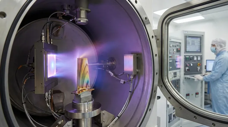
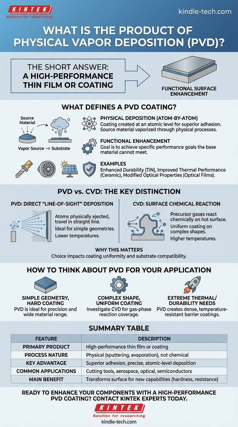
In short, the product of physical vapor deposition (PVD) is a high-performance thin film or coating. This process deposits a very thin layer of source material, often atom by atom, onto the surface of a target object (the substrate). The result is not a standalone product, but a functional surface enhancement that provides specific, engineered properties like hardness, wear resistance, temperature resistance, or unique optical characteristics.
Physical Vapor Deposition does not create a new object; it fundamentally transforms the surface of an existing one. The true product is a high-performance, ultra-thin coating designed to give a component new capabilities it did not originally possess.
What Defines a PVD Coating?
To understand the product of PVD, you must understand its nature. It is fundamentally different from painting or plating because the coating is created at an atomic level, resulting in superior adhesion and performance.
The Product is a Physical Deposition
The name "physical vapor deposition" is critical. The source material is turned into a vapor through a physical process—such as sputtering (bombarding it with high-energy particles) or evaporation (heating it in a vacuum).
These vaporized atoms travel through the vacuum chamber and condense onto the substrate, building a film layer by layer. No fundamental chemical reaction is intended to occur on the part's surface.
The Goal is Functional Enhancement
PVD coatings are applied to achieve a specific performance goal that the base material cannot meet on its own. The product is the function as much as it is the film itself.
Examples from industry include:
- Enhanced Durability: Applying hard, corrosion-resistant coatings of materials like titanium nitride to protect cutting tools and industrial components from wear in harsh environments.
- Improved Thermal Performance: Adding dense, temperature-resistant ceramic coatings to aerospace components, allowing them to withstand extreme heat and operational stress.
- Modified Optical Properties: Depositing precise optical films on solar panels to improve light absorption or on semiconductors as part of the manufacturing process.
Understanding the Key Distinction: PVD vs. CVD
One of the most common points of confusion is the difference between Physical Vapor Deposition (PVD) and Chemical Vapor Deposition (CVD). Understanding this difference clarifies what a PVD product truly is.
PVD: Direct "Line-of-Sight" Deposition
In PVD, atoms are physically ejected from a solid source and travel in a straight line to coat the substrate. Think of it as a highly controlled, atomic-level form of spray painting. The material that lands on the part is the same material that left the source.
CVD: Surface Chemical Reaction
In Chemical Vapor Deposition, the chamber is filled with precursor gases. These gases react chemically on the surface of the hot substrate, and the product of that reaction forms the coating.
Why This Matters for the Final Product
This distinction directly impacts the final coated part. PVD is often a lower-temperature process, making it suitable for a wider range of substrate materials. However, because it is a "line-of-sight" process, coating complex, intricate shapes uniformly can be a challenge.
CVD, by contrast, involves a gas that can flow around the part, making it excellent for creating highly uniform coatings on complex geometries. However, it often requires higher temperatures that the substrate must be able to withstand.
How to Think About PVD for Your Application
Choosing a surface treatment depends entirely on your end goal. The "product" you need is defined by the problem you are trying to solve.
- If your primary focus is adding a hard, wear-resistant, or specific optical coating to a relatively simple geometry: PVD is often the ideal choice due to its precision and the wide range of materials that can be deposited.
- If your primary focus is applying a highly uniform coating over a complex, non-line-of-sight part: You should investigate Chemical Vapor Deposition (CVD), as its gas-phase reaction can cover intricate shapes more effectively.
- If your primary focus is thermal management or durability in extreme environments: PVD is a proven method for creating the dense, temperature-resistant barrier coatings required in demanding fields like aerospace.
Ultimately, view PVD not as a manufacturing process for creating objects, but as a surface engineering tool for unlocking new levels of material performance.
Summary Table:
| Feature | Description |
|---|---|
| Primary Product | A high-performance thin film or coating |
| Process Nature | Physical (sputtering, evaporation), not chemical |
| Key Advantage | Superior adhesion and precise, atomic-level deposition |
| Common Applications | Cutting tools, aerospace components, optical films, semiconductors |
| Main Benefit | Transforms a component's surface to provide new capabilities (e.g., hardness, corrosion resistance) |
Ready to enhance your components with a high-performance PVD coating?
At KINTEK, we specialize in advanced lab equipment and consumables for surface engineering. Our expertise in PVD technology can help you achieve superior wear resistance, thermal performance, and durability for your laboratory or manufacturing needs.
Contact our experts today to discuss how a PVD coating solution can solve your specific material challenges and unlock new levels of performance for your products.
Visual Guide
Related Products
- Chemical Vapor Deposition CVD Equipment System Chamber Slide PECVD Tube Furnace with Liquid Gasifier PECVD Machine
- RF PECVD System Radio Frequency Plasma-Enhanced Chemical Vapor Deposition RF PECVD
- 915MHz MPCVD Diamond Machine Microwave Plasma Chemical Vapor Deposition System Reactor
- HFCVD Machine System Equipment for Drawing Die Nano-Diamond Coating
- Split Chamber CVD Tube Furnace with Vacuum Station Chemical Vapor Deposition System Equipment Machine
People Also Ask
- What are the core advantages of PE-CVD in OLED encapsulation? Protect Sensitive Layers with Low-Temp Film Deposition
- What is plasma enhanced chemical vapor deposition PECVD equipment? A Guide to Low-Temperature Thin Film Deposition
- How are carbon nanotubes grown? Master Scalable Production with Chemical Vapor Deposition
- What types of substrates are used in CVD to facilitate graphene films? Optimize Graphene Growth with the Right Catalyst
- Why is Chemical Vapor Deposition (CVD) equipment uniquely suited for constructing hierarchical superhydrophobic structures?


