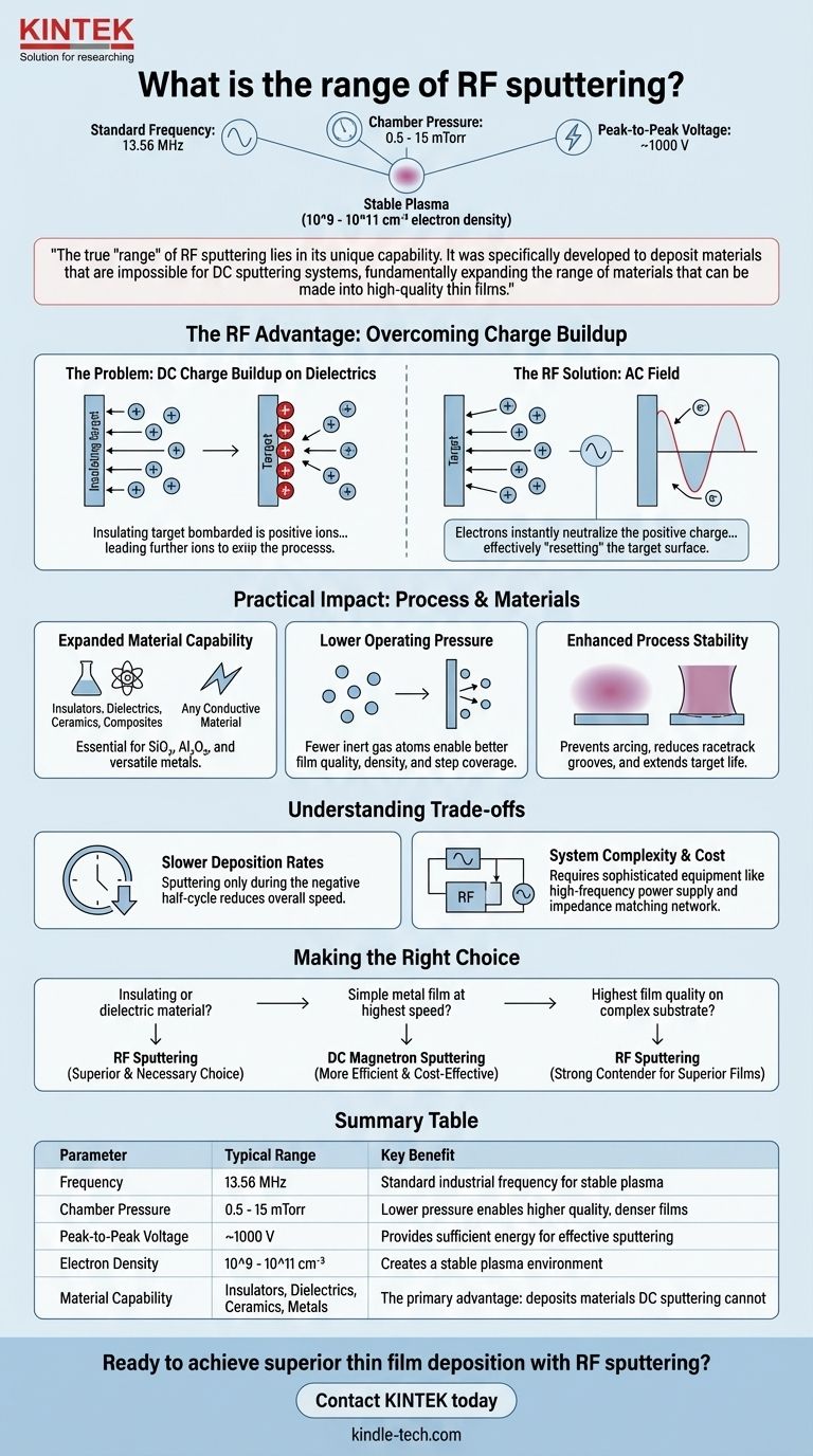
The typical operating range of RF sputtering is defined by a standard industrial frequency of 13.56 MHz, a chamber pressure between 0.5 and 15 mTorr, and a peak-to-peak voltage of around 1000 V. These parameters create a stable plasma with electron densities in the range of 10^9 to 10^11 cm⁻³, suitable for depositing a wide variety of materials.
While the numerical parameters define its operating window, the true "range" of RF sputtering lies in its unique capability. It was specifically developed to deposit materials that are impossible for DC sputtering systems, fundamentally expanding the range of materials that can be made into high-quality thin films.
Why RF Sputtering Excels with Insulators
The core reason for using RF sputtering is to overcome a fundamental limitation of its predecessor, DC sputtering. The problem lies in how electricity interacts with different types of materials.
The Problem: Charge Buildup on Dielectric Targets
In any sputtering process, a target material is bombarded by positive ions from a plasma. To attract these ions, the target is given a strong negative DC voltage.
This works perfectly for conductive metal targets, which can easily replenish the electrons lost to neutralize the incoming positive ions.
However, with an insulating (dielectric) target, this process fails. Positive ions accumulate on the surface, and because the material is an insulator, the charge cannot dissipate. This effect, known as charge-up, quickly neutralizes the negative bias, stops the ion bombardment, and halts the entire sputtering process.
The RF Solution: An Alternating Current Field
RF sputtering solves this by replacing the steady DC voltage with a high-frequency alternating current (AC) field.
In the first half of the AC cycle, the target is negatively charged. This attracts positive ions from the plasma, which strike the target and sputter material just like in a DC system.
In the crucial second half-cycle, the target becomes positively charged. It now repels the positive ions and instead attracts a shower of highly mobile electrons from the plasma. These electrons instantly neutralize the positive charge that built up during the previous cycle, effectively "resetting" the target surface before the next sputtering cycle begins.
The Practical Impact on Process and Materials
This clever use of an AC field has significant consequences for both the types of materials you can use and the quality of the films you can produce.
Expanded Material Capability
The primary benefit of RF sputtering is its ability to deposit insulators, dielectrics, ceramics, and composites. This capability is essential in the semiconductor industry for creating films like silicon dioxide (SiO2) and aluminum oxide (Al2O3).
While it excels with insulators, it can also deposit any conductive material, such as metals and alloys, making it an extremely versatile technique.
Lower Operating Pressure
RF sputtering can sustain a stable plasma at much lower pressures (0.5 - 15 mTorr) than DC systems.
Operating in a higher vacuum means there are fewer inert gas atoms between the target and the substrate. This allows sputtered atoms to travel in a more direct path, leading to better film quality, higher density, and improved step coverage over complex surfaces.
Enhanced Process Stability
The AC field prevents the sudden electrical discharges, known as arcing, that are common when charge builds up. This leads to a more stable and reliable process.
Furthermore, it avoids other issues like the "disappearing anode effect" and promotes more uniform target erosion, reducing the deep "racetrack" grooves seen in some magnetron systems and extending target life.
Understanding the Trade-offs
No technology is without its limitations. To be a truly effective tool, you must understand where RF sputtering might not be the optimal choice.
Slower Deposition Rates
The most significant trade-off is speed. Because the target is only being sputtered during the negative half of the AC cycle, the overall deposition rate is typically lower than that of a comparable DC sputtering process for conductive materials.
System Complexity and Cost
An RF sputtering system requires more sophisticated equipment than a DC system. This includes a high-frequency RF power supply and an impedance matching network to efficiently transfer power to the plasma. This added complexity increases the overall cost and maintenance requirements of the equipment.
Making the Right Choice for Your Application
Selecting the correct deposition technique depends entirely on your material and performance goals.
- If your primary focus is depositing an insulating or dielectric material: RF sputtering is the necessary and superior choice, as it is specifically designed to handle these materials effectively.
- If your primary focus is depositing a simple metal film at the highest possible speed: DC magnetron sputtering is likely a more efficient and cost-effective option due to its significantly higher deposition rates.
- If your primary focus is achieving the highest film quality and uniformity on a complex substrate: RF sputtering is a very strong contender, even for metals, because its stable, low-pressure plasma can produce superior films.
Ultimately, understanding the fundamental principles of RF sputtering allows you to choose the right tool for the job.
Summary Table:
| Parameter | Typical Range | Key Benefit |
|---|---|---|
| Frequency | 13.56 MHz | Standard industrial frequency for stable plasma |
| Chamber Pressure | 0.5 - 15 mTorr | Lower pressure enables higher quality, denser films |
| Peak-to-Peak Voltage | ~1000 V | Provides sufficient energy for effective sputtering |
| Electron Density | 10^9 - 10^11 cm⁻³ | Creates a stable plasma environment |
| Material Capability | Insulators, Dielectrics, Ceramics, Metals | The primary advantage: deposits materials DC sputtering cannot |
Ready to achieve superior thin film deposition with RF sputtering?
Whether your research or production requires depositing challenging dielectric materials like silicon dioxide (SiO₂) or achieving the highest film quality on complex substrates, KINTEK has the expertise and equipment to support your goals. Our range of lab equipment and consumables is designed to meet the precise needs of laboratory professionals.
Contact KINTEK today to discuss how our RF sputtering solutions can expand your material capabilities and enhance your process stability.
Visual Guide
Related Products
- RF PECVD System Radio Frequency Plasma-Enhanced Chemical Vapor Deposition RF PECVD
- Horizontal High Temperature Graphite Vacuum Graphitization Furnace
- Spark Plasma Sintering Furnace SPS Furnace
- Automatic Laboratory Hydraulic Press for XRF & KBR Pellet Press
- Electron Beam Evaporation Coating Oxygen-Free Copper Crucible and Evaporation Boat
People Also Ask
- How does plasma enhance CVD? Unlock Low-Temperature, High-Quality Film Deposition
- What is plasma chemical vapor deposition? A Low-Temperature Thin Film Coating Solution
- How does Radio Frequency Enhanced Plasma Chemical Vapour Deposition (RF-PECVD) work? Learn the Core Principles
- What is the role of RF-PECVD in VFG preparation? Mastering Vertical Growth and Surface Functionality
- Why is a Matching Network Indispensable in RF-PECVD for Siloxane Films? Ensure Stable Plasma and Uniform Deposition


