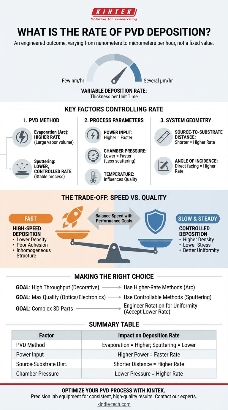
The deposition rate for Physical Vapor Deposition (PVD) is not a single, fixed value but a highly variable parameter that can range from a few nanometers to several micrometers per hour. The specific rate is entirely dependent on the chosen PVD method, the material being deposited, and the precise operating parameters of the system.
The critical insight is that PVD deposition rate is not a number you look up, but an outcome you engineer. Understanding the factors that control this rate is fundamental to achieving your desired coating thickness, quality, and manufacturing throughput.
What is Deposition Rate?
Deposition rate is the measure of how quickly a thin film grows on a substrate during the PVD process. It is typically expressed as thickness per unit of time, such as nanometers per minute (nm/min) or micrometers per hour (µm/hr).
This rate is one of the most critical process parameters. It directly influences not only the time required to manufacture a part but also the final properties of the coating, such as its density, adhesion, and internal stress.
Key Factors Controlling PVD Rate
The rate of deposition is a result of several interconnected variables. Controlling these factors is the key to a repeatable and successful PVD process.
Factor 1: The PVD Method
The underlying physics of the deposition method is the primary determinant of the potential rate.
- Evaporation (e.g., Arc Deposition): In methods like arc vapor deposition, a source material is heated until it evaporates, creating a vapor that condenses on the substrate. These processes are generally higher-rate because they can generate a large volume of vapor material quickly.
- Sputtering: In sputtering, high-energy ions bombard a source material (target), physically knocking atoms off its surface. These ejected atoms then travel to the substrate. Sputtering is typically a lower-rate but more controlled and stable process compared to evaporation.
Factor 2: Process Parameters
For any given method, the operator has direct control over parameters that fine-tune the rate.
- Power Input: This is the most direct control. Increasing the power to an arc source or a sputtering cathode will increase the rate of evaporation or sputtering, respectively, leading to a faster deposition rate.
- Chamber Pressure: The pressure of the background or reactive gas inside the chamber affects how efficiently material travels from the source to the substrate. Too high a pressure can cause vapor atoms to scatter, reducing the deposition rate.
- Temperature: Substrate temperature can influence how atoms stick to the surface and the resulting film density. While it has a less direct impact on rate than power, it is a critical factor for film quality.
Factor 3: System Geometry
The physical layout of the PVD chamber plays a significant and often overlooked role.
- Source-to-Substrate Distance: The closer the substrate is to the deposition source, the higher the rate of deposition will be. The flux of depositing material decreases with the square of the distance.
- Angle of Incidence: Parts of a substrate directly facing the source will have a much higher deposition rate than surfaces at a steep angle. This is why complex parts are often rotated on multi-axis fixtures to ensure uniform coating.
Understanding the Trade-offs: Speed vs. Quality
Simply maximizing the deposition rate is rarely the best strategy, as it almost always involves a compromise in coating quality.
The Cost of High-Speed Deposition
Pushing for the fastest possible rate can lead to significant defects in the coating.
- Lower Density: Rapidly arriving atoms have less time to settle into an ordered, dense film structure, which can result in a more porous coating.
- Poor Adhesion: A very high deposition rate can create internal stresses in the film, leading to poor adhesion and potential flaking.
- Inhomogeneous Structure: The film's microstructure and properties can become less uniform when deposited too quickly.
The Benefit of Slow, Controlled Deposition
Slower, more deliberate deposition provides a more stable process and often results in superior film properties.
- Higher Density: Atoms have more time and energy to arrange themselves into a dense, non-porous structure, improving barrier and mechanical properties.
- Lower Stress: A slower buildup of material typically results in lower internal stress, which is critical for coating adhesion and long-term performance.
- Better Uniformity: Slower rates are easier to control across a large area or on complex parts, leading to more uniform thickness and properties.
Making the Right Choice for Your Goal
Your optimal deposition rate is determined by your primary objective.
- If your primary focus is high throughput for decorative or low-stress coatings: Favor higher-rate methods like arc evaporation and tune your power settings for maximum speed while monitoring for basic adhesion.
- If your primary focus is maximum film quality for precision optics or electronics: Use a more controllable method like sputtering and prioritize a slow, stable rate to achieve superior density and uniformity.
- If your primary focus is coating complex 3D parts: Acknowledge that the effective rate will vary across the part's surface and engineer a rotation and movement plan that prioritizes uniformity, often accepting a lower overall average rate.
Ultimately, mastering the PVD process means treating deposition rate as a deliberate choice to balance manufacturing speed with final coating performance.
Summary Table:
| Factor | Impact on Deposition Rate |
|---|---|
| PVD Method | Evaporation (e.g., Arc) = Higher Rate; Sputtering = Lower, Controlled Rate |
| Power Input | Higher Power = Faster Rate |
| Source-to-Substrate Distance | Shorter Distance = Higher Rate |
| Chamber Pressure | Lower Pressure = Typically Higher Rate (Less Scattering) |
Ready to Optimize Your PVD Process?
Achieving the perfect balance between deposition speed and coating quality is critical for your project's success. The right lab equipment is the foundation of this control.
KINTEK specializes in precision lab equipment and consumables, providing the reliable tools you need to:
- Precisely control deposition parameters for consistent, high-quality results.
- Scale your process from R&D to production with confidence.
- Coat complex parts uniformly with the right fixturing solutions.
Don't leave your coating performance to chance. Let our experts help you select the ideal equipment for your specific PVD goals.
Contact our team today to discuss your application and discover how KINTEK can enhance your laboratory's capabilities.
Visual Guide
Related Products
- RF PECVD System Radio Frequency Plasma-Enhanced Chemical Vapor Deposition RF PECVD
- Split Chamber CVD Tube Furnace with Vacuum Station Chemical Vapor Deposition System Equipment Machine
- Chemical Vapor Deposition CVD Equipment System Chamber Slide PECVD Tube Furnace with Liquid Gasifier PECVD Machine
- VHP Sterilization Equipment Hydrogen Peroxide H2O2 Space Sterilizer
- Molybdenum Tungsten Tantalum Special Shape Evaporation Boat
People Also Ask
- How does RF power create plasma? Achieve Stable, High-Density Plasma for Your Applications
- What are the benefits of PECVD? Achieve Superior Low-Temperature Thin Film Deposition
- What are the applications of PECVD? Essential for Semiconductors, MEMS, and Solar Cells
- How are PECVD and CVD different? A Guide to Choosing the Right Thin-Film Deposition Process
- Why is PECVD environment friendly? Understanding the Eco-Friendly Benefits of Plasma-Enhanced Coating