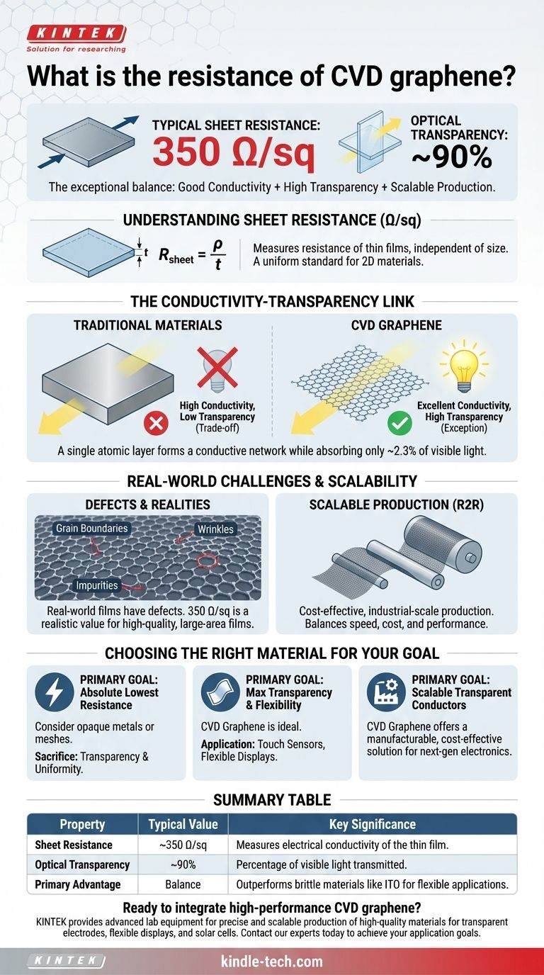
The typical sheet resistance of graphene produced via chemical vapor deposition (CVD) is approximately 350 Ω/sq (ohms per square). This value is achieved while maintaining a high optical transparency of around 90%, a combination that is critical for its use in applications like transparent electrodes and flexible electronics.
The specific resistance value of CVD graphene is less important than the context it exists in. Its true value lies in the exceptional balance it strikes between good electrical conductivity, elite optical transparency, and the potential for cost-effective, large-scale production.
Understanding Sheet Resistance in Graphene
To properly evaluate CVD graphene, we must first understand the metric used to measure its conductivity. The value of 350 Ω/sq is not an arbitrary number; it reflects the material's fundamental properties as a two-dimensional film.
What is Sheet Resistance (Ω/sq)?
Sheet resistance is the standard measure for the resistivity of thin films, including single-layer materials like graphene. Unlike bulk resistance (measured in Ω·m), it's expressed in ohms per square (Ω/sq).
This unit simplifies calculations by normalizing resistance for any square-shaped area of the film, regardless of its physical size. It effectively measures the resistance of a material at a uniform thickness.
The Significance of the CVD Value
A sheet resistance of 350 Ω/sq is highly competitive for a material that is also over 90% transparent. While it's not as conductive as opaque metals, it is an excellent figure for a transparent conductor that is also atomically thin, flexible, and strong.
This performance positions CVD graphene as a leading next-generation alternative to traditional materials like Indium Tin Oxide (ITO), which is more brittle and expensive.
How the CVD Process Achieves This Quality
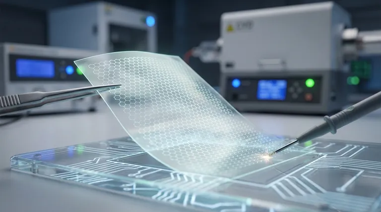
Chemical Vapor Deposition (CVD) is a method that grows a large, continuous, single-layer sheet of graphene on a substrate, typically a copper foil.
The process aims to create a pure and uniform film over a large area. This uniformity is crucial for ensuring consistent electrical properties across the entire surface, preventing "hot spots" or areas of high resistance.
The Critical Link: Resistance and Transparency
The primary reason CVD graphene generates so much interest is its ability to solve a fundamental trade-off in materials science: conductivity versus transparency.
The Inherent Conflict
For most materials, increasing electrical conductivity means decreasing optical transparency. As you add more conductive material (e.g., making a metal film thicker), it inevitably blocks more light.
Why Graphene is an Exception
As a true two-dimensional material, a single layer of graphene forms a continuous conductive network while being almost invisible, absorbing only ~2.3% of visible light.
The ability to achieve 90% transparency, as cited for CVD films, means that the graphene layer and its substrate are allowing the vast majority of light to pass through while still providing an effective path for electrical current.
The Goal: Transparent Conductive Films
This unique combination of properties makes CVD graphene ideal for transparent conductive films (TCFs). These are essential components in devices like touch screens, OLED displays, flexible electronics, and solar cells, where you need to move electricity across a surface without blocking light.
Understanding the Trade-offs and Realities
While the specifications are impressive, it's important to understand the practical limitations and production realities that influence the final performance of CVD graphene.
The Impact of Defects
The goal of CVD is to produce a "perfect" single layer, but real-world films contain defects. Grain boundaries (where different crystalline domains of graphene meet), wrinkles, and impurities introduced during the transfer process can all increase the sheet resistance above theoretical minimums.
The 350 Ω/sq figure represents a realistic value for high-quality, large-area films, not a flawless theoretical sample.
Scalability vs. Perfection
The CVD process is highly valuable because it is scalable, with roll-to-roll (R2R) manufacturing making cost-effective, industrial-scale production possible.
However, high-throughput production can sometimes introduce more defects than slower, lab-scale processes. There is often a trade-off between the cost and speed of production and the ultimate electrical performance of the film.
Balancing Multiple Properties
CVD is a versatile coating technique that can enhance properties like wear resistance, thermal stability, and electrical conductivity. For a single atomic layer of graphene, however, the primary benefits are its unique electrical and optical characteristics, not its mechanical durability compared to thicker coatings.
Making the Right Choice for Your Application
Whether CVD graphene is the correct material depends entirely on your primary engineering goal.
- If your primary focus is the absolute lowest resistance: You may need to consider opaque metal films or transparent metallic meshes, but you will sacrifice significant optical transparency or uniformity.
- If your primary focus is maximum transparency and flexibility: CVD graphene is a leading candidate, as its resistance is more than sufficient for applications like capacitive touch sensors and flexible displays.
- If your primary focus is scalable production of transparent conductors: The roll-to-roll potential of the CVD process makes graphene a cost-effective and highly manufacturable choice for next-generation electronics.
Ultimately, CVD graphene's utility is defined by its unique and powerful combination of good conductivity, excellent transparency, and manufacturing scalability.
Summary Table:
| Property | Typical Value for CVD Graphene | Key Significance |
|---|---|---|
| Sheet Resistance | ~350 Ω/sq | Measures electrical conductivity of the thin film. |
| Optical Transparency | ~90% | Percentage of visible light transmitted. |
| Primary Advantage | Excellent conductivity-transparency balance | Outperforms brittle materials like ITO for flexible applications. |
Ready to integrate high-performance CVD graphene into your next-generation devices?
KINTEK specializes in providing advanced lab equipment and consumables for materials science and electronics R&D. Whether you are developing transparent electrodes, flexible displays, or solar cells, our solutions support the precise and scalable production of high-quality materials.
Contact our experts today to discuss how we can help you achieve your specific application goals with reliable and efficient laboratory technology.
Visual Guide
Related Products
- Laboratory CVD Boron Doped Diamond Materials
- CVD Diamond Wire Drawing Die Blanks for Precision Applications
- CVD Diamond for Thermal Management Applications
- CVD Diamond Dressing Tools for Precision Applications
- Custom CVD Diamond Coating for Lab Applications
People Also Ask
- What is the purpose of performing anodic polarization on BDD electrodes? Ensure Accurate & Reproducible Research Results
- Are CVD diamonds synthetic? Discover the Truth About Lab-Grown Diamonds
- What is the demand of CVD diamonds? Driven by Ethics, Purity, and Affordability
- How much cheaper are CVD diamonds? Save 20-30% on a Genuine Diamond
- What are the applications of CVD diamonds? From Jewelry to High-Tech Tools


