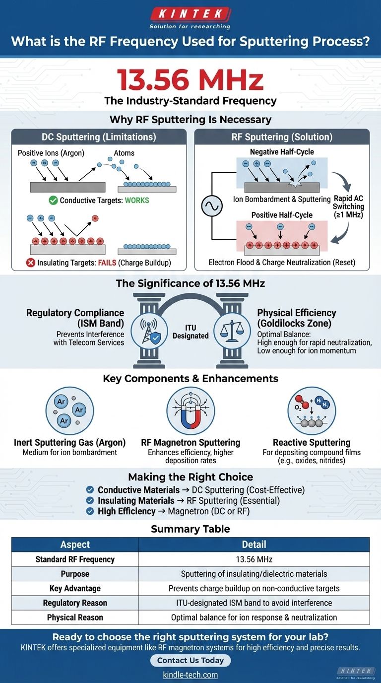
For RF sputtering, the industry-standard frequency used is 13.56 MHz. This specific frequency is chosen because it is designated for Industrial, Scientific, and Medical (ISM) applications, which prevents interference with telecommunication services, while also being physically effective for the sputtering process.
The core challenge in thin-film deposition is sputtering materials that do not conduct electricity. RF sputtering solves this by using a high-frequency alternating voltage, with 13.56 MHz being the standard, to prevent charge buildup that would otherwise halt the process.
Why RF Sputtering Is Necessary
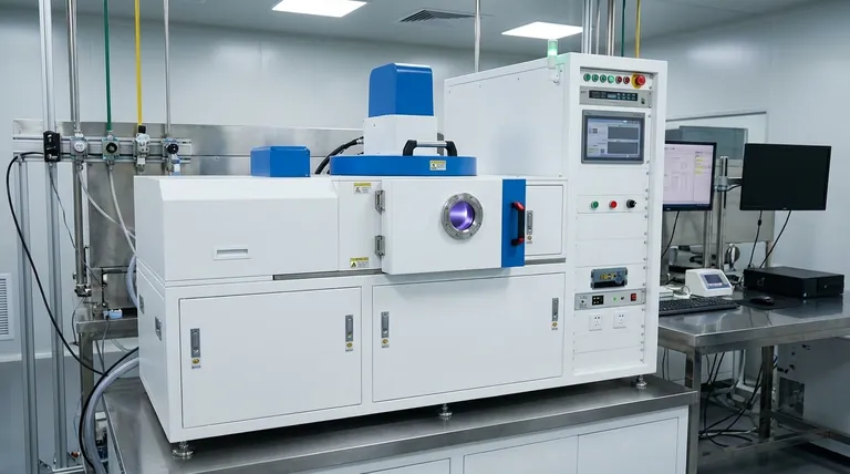
In sputtering, we bombard a source material (the "target") with energized ions to eject atoms, which then deposit as a thin film on a substrate. The method used to energize these ions depends on the target's electrical properties.
The Limitation of DC Sputtering
For conductive targets, a simple DC voltage works perfectly. A negative voltage is applied to the target, attracting positive ions (like Argon) from the plasma, which strike the target and sputter away material.
This method fails for insulating targets. Positive ions striking the insulator build up a positive charge on its surface. This charge repels any more incoming positive ions, effectively stopping the sputtering process almost immediately.
How RF Solves the Charge Buildup Problem
RF (Radio Frequency) sputtering overcomes this by applying a high-frequency alternating voltage. This AC field rapidly switches the target's polarity.
In the negative half-cycle, positive ions are attracted to and bombard the target, just like in DC sputtering.
In the positive half-cycle, the target attracts a flood of highly mobile electrons from the plasma. This instantly neutralizes the positive charge built up during the previous cycle, "resetting" the target surface for the next round of ion bombardment. This cycle must occur at a frequency of 1 MHz or higher to be effective.
The Significance of 13.56 MHz
While any frequency above 1 MHz can work, the choice of 13.56 MHz is not arbitrary. It represents a balance between regulatory compliance and physical efficiency.
An ITU-Designated ISM Band
The International Telecommunication Union (ITU) reserves specific frequencies for Industrial, Scientific, and Medical (ISM) use.
Using the 13.56 MHz band ensures that the powerful radio signals generated by the sputtering equipment do not interfere with critical communication and broadcast services.
A "Goldilocks" Frequency for Sputtering
This frequency is also in a sweet spot for the physics of the process. It is high enough to enable the rapid charge neutralization required for insulating targets.
At the same time, it is low enough that the heavier ions (like Argon) can still respond to the electric field and gain sufficient momentum to effectively sputter the target.
Key Components of the Sputtering Environment
The RF power source is just one part of a complete system. Two other elements are critical for a successful deposition.
The Inert Sputtering Gas
The process requires a medium of ions to bombard the target. This is almost always an inert gas, chosen because it will not chemically react with the target material.
Argon (Ar) is the most common choice due to its relatively high atomic mass and cost-effectiveness. The argon atoms are ionized in the plasma, accelerated toward the target, and do the physical work of sputtering.
Enhancing Efficiency with Magnetrons
RF Magnetron Sputtering is an enhancement that dramatically improves a system's efficiency. It uses a powerful magnetic field configured behind the target.
This magnetic field traps electrons in a "magnetic tunnel" near the target surface. These trapped electrons increase the probability of collisions with argon atoms, creating more ions for sputtering. This allows the process to run at lower pressures with higher deposition rates.
Understanding the Trade-offs
While RF sputtering is a versatile and powerful technique, it is not without its complexities and is not always the necessary choice.
Capability vs. Complexity
The primary advantage of RF sputtering is its ability to deposit insulating and dielectric materials. This capability is impossible with simpler DC systems.
However, RF power supplies, matching networks, and the associated shielding are significantly more complex and expensive than their DC counterparts. This adds to the overall cost and maintenance burden of the equipment.
Reactive Sputtering
In some cases, a reactive gas like nitrogen or oxygen is intentionally added to the argon. This process, known as reactive sputtering, allows the sputtered metal atoms to react with the gas mid-flight or on the substrate. This is a common method for depositing compound films like titanium nitride (TiN) or aluminum oxide (Al2O3).
Making the Right Choice for Your Goal
Selecting the right sputtering technique depends entirely on the material you need to deposit and your performance requirements.
- If your primary focus is depositing conductive materials (metals): A simpler and more cost-effective DC sputtering system is often the superior choice.
- If your primary focus is depositing insulating materials (ceramics, oxides): RF sputtering is not just an option; it is a necessity.
- If your primary focus is achieving high deposition rates or process efficiency: Incorporating magnetrons into either your DC or RF system is the most effective strategy.
Ultimately, understanding these core principles empowers you to choose the correct tool for your specific material-deposition challenge.
Summary Table:
| Aspect | Detail |
|---|---|
| Standard RF Frequency | 13.56 MHz |
| Purpose | Sputtering of insulating/dielectric materials |
| Key Advantage | Prevents charge buildup on non-conductive targets |
| Regulatory Reason | ITU-designated ISM band to avoid interference |
| Physical Reason | Optimal balance for ion response and charge neutralization |
Ready to choose the right sputtering system for your lab's specific material-deposition challenges?
Whether you need to deposit conductive metals with a cost-effective DC system or require the advanced capability of an RF system for insulating ceramics and oxides, KINTEK has the expertise and equipment to support your research and production goals. Our specialized lab equipment, including RF magnetron sputtering systems, is designed to deliver high efficiency and precise results.
Contact us today via our [#ContactForm] to discuss your project and discover how KINTEK's solutions can enhance your thin-film deposition processes.
Visual Guide
Related Products
- RF PECVD System Radio Frequency Plasma-Enhanced Chemical Vapor Deposition RF PECVD
- Spark Plasma Sintering Furnace SPS Furnace
- Horizontal High Temperature Graphite Vacuum Graphitization Furnace
People Also Ask
- What is plasma CVD? Unlock Low-Temperature Thin Film Deposition for Sensitive Materials
- What is plasma chemical vapor deposition? A Low-Temperature Thin Film Coating Solution
- What is the role of RF-PECVD in VFG preparation? Mastering Vertical Growth and Surface Functionality
- How does Radio Frequency Enhanced Plasma Chemical Vapour Deposition (RF-PECVD) work? Learn the Core Principles
- What is plasma enhanced chemical Vapour deposition process used for fabrication of? A Guide to Low-Temperature Thin Films


