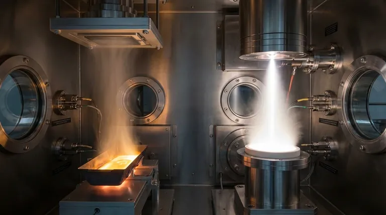
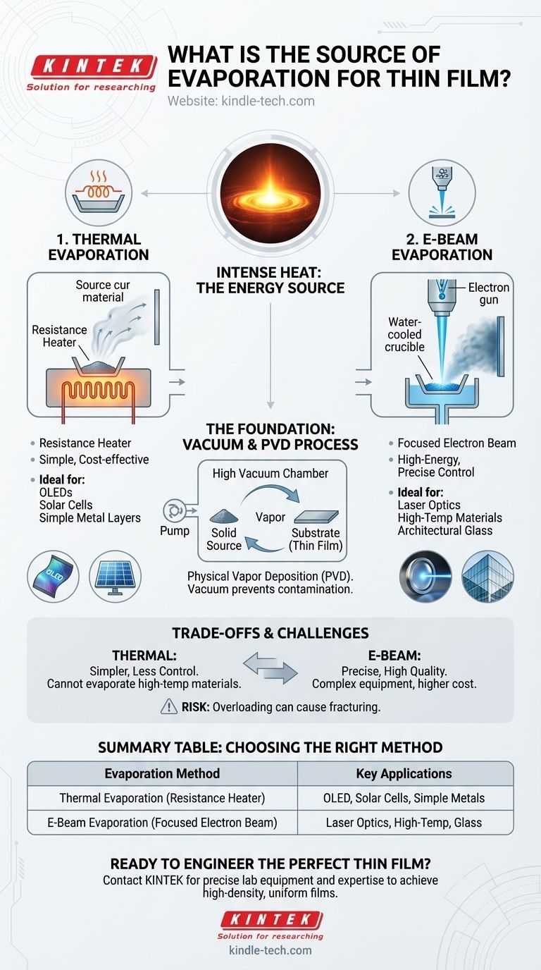
In thin film deposition, the source of evaporation is always intense heat. This energy is delivered through one of two primary methods: directly heating a container holding the source material, known as thermal evaporation, or bombarding the material with a focused, high-energy beam of electrons, known as electron beam (e-beam) evaporation.
The core challenge in creating a thin film is turning a solid source material into a vapor that can then condense onto a surface. The choice between using a simple resistance heater or a high-precision electron beam is the fundamental decision that dictates the quality, properties, and application of the final film.
The Foundation: Evaporation in a Vacuum
The Core Principle: A Simple Phase Change
Evaporation is a form of Physical Vapor Deposition (PVD). At its heart, the process is a simple transition from a solid to a gaseous state and back to a solid.
A source material is heated in a high vacuum until it turns into a vapor. This vapor then travels and condenses onto a cooler surface, called a substrate, forming a uniform, solid thin film.
Why a Vacuum is Non-Negotiable
This entire process must occur in a high-vacuum chamber. The vacuum removes air and other particles that could contaminate the film or interfere with the vaporized material's path to the substrate.
The Two Primary Evaporation Sources
Method 1: Thermal Evaporation
Thermal evaporation is the most straightforward PVD method. The source material is placed in a small container, often a tungsten "boat" or filament.
An electric current is passed through this container, acting as a resistance heater. This raises the temperature significantly, causing the source material to melt and then evaporate into a vapor.
This method is highly effective for depositing pure metals, non-metals, and certain oxides. It is widely used for creating electrically conductive layers for OLED displays, solar cells, and thin-film transistors.
Method 2: Electron Beam (E-Beam) Evaporation
E-beam evaporation uses a more complex and powerful energy source. A high-energy beam of electrons is generated and magnetically guided to strike the surface of the source material.
This focused energy transfer is incredibly efficient, allowing for the evaporation of materials with very high melting points that are inaccessible with standard thermal evaporation.
The precision of the electron beam results in high-density thin films with superior adhesion to the substrate. This control makes it ideal for advanced applications like precision laser optics and high-performance architectural glass.
Understanding the Trade-offs and Challenges
Simplicity vs. Control
Thermal evaporation is simpler and generally less expensive to implement. However, it offers less control over the evaporation rate and can be less uniform.
E-beam evaporation provides precise control over the energy input, enabling a more consistent deposition rate and higher-quality films, but the equipment is more complex.
Material Compatibility
The choice of source is often dictated by the material itself. While thermal evaporation works well for many common metals, it cannot reach the temperatures required to evaporate refractory metals or certain ceramics.
E-beam is the definitive choice for these high-temperature materials, as the localized energy of the beam can vaporize almost any substance.
Common Process Risks
Regardless of the method, operators must carefully manage the amount of source material. Overloading a container can lead to particle fracturing or even explosive reactions under the intense heat and vacuum.
Additionally, some complex materials can decompose or react chemically during heating, altering the composition of the final film.
Making the Right Choice for Your Goal
Ultimately, the correct evaporation source depends entirely on the desired outcome and the material being used.
- If your primary focus is creating simple conductive metal layers: Thermal evaporation is often the most direct and cost-effective method.
- If your primary focus is high-purity, high-density films or optical coatings: E-beam evaporation provides the necessary control and energy for superior results.
- If your primary focus is depositing materials with extremely high melting points: E-beam evaporation is the only viable choice.
Choosing the right energy source is the first step in engineering the precise characteristics of your thin film.
Summary Table:
| Evaporation Method | Energy Source | Key Applications |
|---|---|---|
| Thermal Evaporation | Resistance Heater (e.g., Tungsten Boat) | OLED Displays, Solar Cells, Simple Metal Layers |
| E-Beam Evaporation | Focused Electron Beam | Laser Optics, High-Temperature Materials, Architectural Glass |
Ready to engineer the perfect thin film for your application? The choice between thermal and e-beam evaporation is critical for achieving the desired film properties, from simple conductive layers to high-purity optical coatings. At KINTEK, we specialize in providing the precise lab equipment and consumables needed for your thin film deposition processes. Our experts can help you select the right evaporation source to ensure high-density, uniform films with superior adhesion. Contact us today to discuss your project requirements and discover how KINTEK can enhance your laboratory's capabilities. Get in touch via our Contact Form
Visual Guide
Related Products
- Aluminized Ceramic Evaporation Boat for Thin Film Deposition
- Tungsten Evaporation Boat for Thin Film Deposition
- Molybdenum Tungsten Tantalum Evaporation Boat for High Temperature Applications
- Electron Beam Evaporation Coating Oxygen-Free Copper Crucible and Evaporation Boat
- Hemispherical Bottom Tungsten Molybdenum Evaporation Boat
People Also Ask
- What are thin films deposited by evaporation? A Guide to High-Purity Coating
- What are the alternatives to sputtering? Choose the Right Thin Film Deposition Method
- Why is an alumina boat selected for catalyst precursors? Ensure Sample Purity at 1000 °C
- Why is an alumina boat and Ti3AlC2 powder bed necessary for Ti2AlC sintering? Protect MAX Phase Purity
- What are the applications of thin films deposition? Unlock New Possibilities for Your Materials


