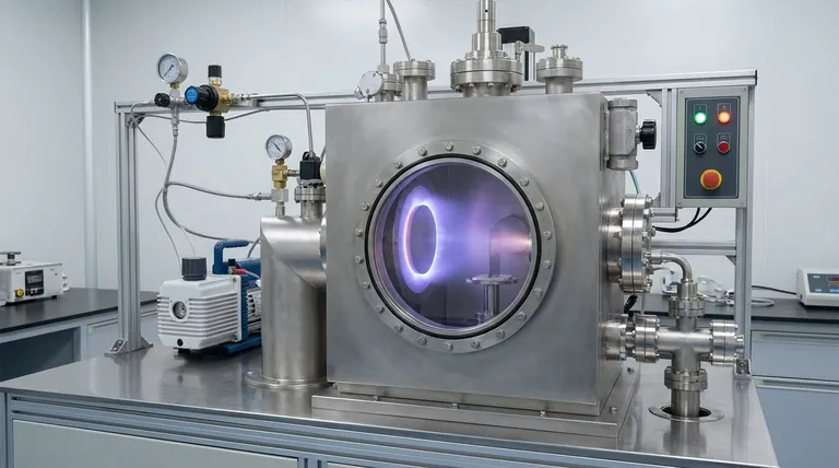
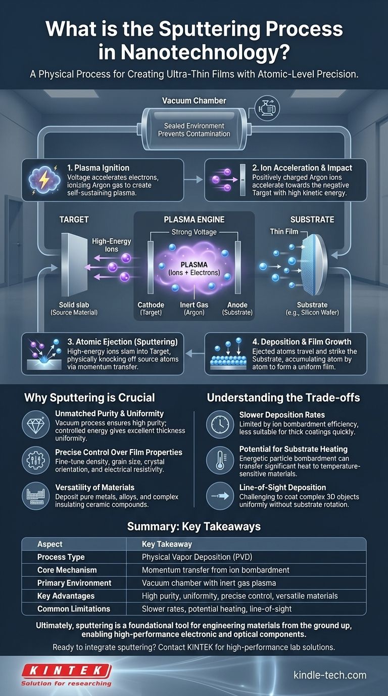
At its core, sputtering is a physical process used to create ultra-thin films of material with atomic-level precision. Inside a vacuum, high-energy ions are used to bombard a source material, known as a target. This bombardment physically knocks atoms off the target's surface, which then travel and deposit onto a substrate, building a new film one atomic layer at a time.
Sputtering is not merely a coating technique; it is a fundamental tool for engineering materials from the ground up. Its true value in nanotechnology lies in the exceptional control it provides over a film's purity, density, and structure, making it indispensable for creating high-performance electronic and optical components.
Deconstructing the Sputtering Environment
To understand the process, we must first understand its highly controlled setting. Sputtering takes place inside a sealed vacuum chamber where every element has a distinct role.
The Vacuum Chamber
The entire process occurs in a vacuum to prevent contamination. Removing air and other particles ensures that the sputtered atoms do not collide with unwanted molecules on their way to the substrate, guaranteeing a film of the highest possible purity.
The Key Players: Target, Substrate, and Gas
The chamber contains three critical components. The target is a solid slab of the source material you wish to deposit. The substrate is the object you are coating, such as a silicon wafer or piece of glass. Finally, an inert gas, most commonly Argon, is introduced into the chamber in small, controlled amounts.
The Plasma Engine
A strong voltage is applied between the target and the substrate, making the target a negative electrode (cathode). This voltage energizes free electrons, which collide with the neutral Argon atoms. These collisions knock electrons off the Argon atoms, creating a cloud of positively charged Argon ions and free electrons known as a plasma.
The Step-by-Step Atomic Bombardment
With the environment set, the sputtering process unfolds as a precise, four-step sequence of events driven by physics.
Step 1: Plasma Ignition
The electric field within the chamber accelerates free electrons, causing them to collide with and ionize the Argon gas atoms. This creates the self-sustaining plasma that serves as the engine for the entire process.
Step 2: Ion Acceleration and Impact
The newly formed, positively charged Argon ions are powerfully attracted to the negatively charged target. They accelerate across the chamber, gaining significant kinetic energy.
Step 3: Atomic Ejection (Sputtering)
These high-energy ions slam into the target's surface. This is not a chemical reaction but a pure momentum transfer, like a cue ball striking a rack of billiard balls. The impact sets off a collision cascade within the target material, and when this cascade reaches the surface, it ejects individual atoms.
Step 4: Deposition and Film Growth
The ejected atoms from the target travel through the vacuum chamber and strike the substrate. They stick to its surface, gradually accumulating to form a thin, uniform, and dense film.
Why Sputtering is Crucial for Nanotechnology
Sputtering is more complex than other deposition methods, but its adoption in nanotechnology is due to its distinct and powerful advantages.
Unmatched Purity and Uniformity
Because it is a physical process that occurs in a vacuum, sputtering produces exceptionally pure films. The line-of-sight deposition and controlled energy result in films with outstanding thickness uniformity across the entire substrate.
Precise Control Over Film Properties
Sputtering allows for fine-tuning of a film’s final characteristics. By adjusting parameters like gas pressure, voltage, and temperature, engineers can precisely control the film's density, grain size, crystal orientation, and electrical resistivity.
Versatility of Materials
The process is incredibly versatile and can be used to deposit a vast range of materials. This includes pure metals, alloys, and even insulating ceramic compounds that are difficult or impossible to deposit using heat-based evaporation methods.
Understanding the Trade-offs
No technique is without its limitations. Objectivity requires acknowledging the trade-offs associated with sputtering.
Slower Deposition Rates
Sputtering is generally a slower process compared to thermal evaporation. The rate of material ejection is limited by the ion bombardment efficiency, making it less suitable for applications requiring very thick coatings quickly.
Potential for Substrate Heating
The constant bombardment of energetic particles (both sputtered atoms and ions) can transfer significant heat to the substrate. This can be problematic when coating temperature-sensitive materials like certain plastics or biological samples.
Line-of-Sight Deposition
The sputtered atoms travel in a straight line from the target to the substrate. This can make it challenging to achieve a uniform coating on complex, three-dimensional objects without sophisticated machinery to rotate the substrate during deposition.
Making the Right Choice for Your Goal
Selecting a deposition technique depends entirely on the desired outcome for your film.
- If your primary focus is high-purity, dense, and uniform films for electronics or optics: Sputtering is the superior choice due to its controlled, physical deposition mechanism.
- If your primary focus is coating complex, non-planar shapes: You must account for sputtering's line-of-sight nature and incorporate substrate rotation to ensure even coverage.
- If your primary focus is speed and low cost for simple coatings: You might consider thermal evaporation, but be prepared to sacrifice the film quality, density, and control that sputtering provides.
Ultimately, sputtering is a foundational manufacturing process that empowers engineers to build high-value materials with atomic-scale precision.
Summary Table:
| Aspect | Key Takeaway |
|---|---|
| Process Type | Physical Vapor Deposition (PVD) |
| Core Mechanism | Momentum transfer from ion bombardment to eject target atoms |
| Primary Environment | Vacuum chamber with inert gas (e.g., Argon) plasma |
| Key Advantages | High purity, excellent uniformity, precise control over film properties, versatile material compatibility |
| Common Limitations | Slower deposition rates, potential for substrate heating, line-of-sight deposition |
Ready to integrate sputtering into your R&D or production line? KINTEK specializes in high-performance lab equipment and consumables for nanotechnology. Our sputtering systems are engineered to deliver the precision, purity, and control your laboratory demands for creating next-generation electronic and optical components. Contact our experts today to discuss how we can help you achieve superior thin-film results.
Visual Guide
Related Products
- Spark Plasma Sintering Furnace SPS Furnace
- Vacuum Induction Melting Spinning System Arc Melting Furnace
- Chemical Vapor Deposition CVD Equipment System Chamber Slide PECVD Tube Furnace with Liquid Gasifier PECVD Machine
- Customer Made Versatile CVD Tube Furnace Chemical Vapor Deposition Chamber System Equipment
People Also Ask
- What is the difference between spark plasma sintering and flash sintering? A Guide to Advanced Sintering Methods
- What are the advantages of CAMI/SPS for W-Cu composite preparation? Reduce cycles from hours to seconds.
- Why are Spark Plasma Sintering (SPS) furnaces or hot presses utilized in the preparation of Li3PS4 solid electrolytes?
- What is SPS sintering method? A Guide to High-Speed, High-Performance Material Fabrication
- What is the theory of spark plasma sintering? A Guide to Rapid, Low-Temperature Densification


