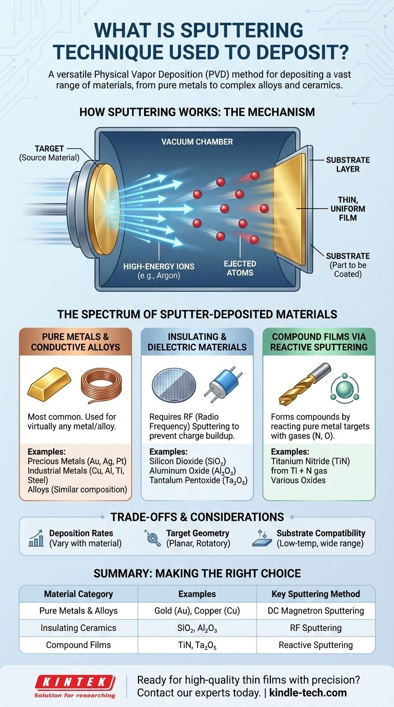
At its core, the sputtering technique is a physical vapor deposition (PVD) method capable of depositing an exceptionally wide range of materials. This includes nearly any solid element, from pure metals like gold and copper to complex alloys and advanced ceramic compounds like oxides and nitrides, onto a substrate.
Sputtering is not defined by a limited set of materials but by its physical process: the bombardment of a source 'target' to eject atoms. This fundamental mechanism makes it one of the most versatile and controllable thin-film deposition techniques available for coating surfaces.
How Sputtering Works: A Primer
Sputtering is a vacuum-based process that offers atomic-level control over film deposition. The mechanics behind its versatility are straightforward.
The Basic Mechanism
In a vacuum chamber, a substrate (the part to be coated) is placed opposite a "target" made of the desired coating material. High-energy ions, typically from an inert gas like Argon, are accelerated and collide with the target.
These collisions are energetic enough to physically knock atoms loose from the target material. These ejected atoms then travel through the vacuum and condense onto the substrate, building up a thin, uniform film.
The Spectrum of Sputter-Deposited Materials
The true power of sputtering lies in the sheer breadth of materials it can handle. By modifying the process, we can deposit conductors, insulators, and complex chemical compounds with high precision.
Pure Metals and Conductive Alloys
This is the most common application of sputtering. Because the process is purely physical, it can be used to deposit virtually any metal or electrically conductive alloy.
Common examples include:
- Precious Metals: Gold (Au), Silver (Ag), Platinum (Pt)
- Industrial Metals: Copper (Cu), Aluminum (Al), Titanium (Ti), Steel
- Alloys: By using a target made of a pre-formed alloy, the resulting film will have a highly similar chemical composition.
Insulating and Dielectric Materials
Depositing electrically insulating materials requires a specific variation called RF (Radio Frequency) Sputtering. A standard DC power source would cause a positive charge to build up on an insulating target, halting the process.
RF sputtering alternates the electric field at high frequency, neutralizing this charge buildup and allowing for the deposition of ceramics and dielectrics such as Silicon Dioxide (SiO₂), Aluminum Oxide (Al₂O₃), and Tantalum Pentoxide (Ta₂O₅).
Compound Films via Reactive Sputtering
Reactive sputtering is an elegant method for forming compounds that may be difficult to produce as a stable target. Instead of using a compound target, a pure metal target is used in a reactive gas atmosphere.
For example, by sputtering a Titanium (Ti) target in an environment containing nitrogen gas, the sputtered titanium atoms react with the nitrogen to form a Titanium Nitride (TiN) film on the substrate. The same principle applies to creating oxides by introducing oxygen.
Understanding the Trade-offs and Considerations
While incredibly versatile, sputtering is a precision process with factors that must be managed to achieve the desired outcome.
Deposition Rates and Efficiency
Different materials have different "sputter yields," meaning they eject atoms at different rates under the same conditions. This affects the time and power required to achieve a desired film thickness.
Target Material and Geometry
The source material, or target, comes in different forms. Planar targets are flat plates used in large-scale systems, while rotatory targets are cylindrical and used to achieve high uniformity and material utilization in other system designs.
Substrate Compatibility
One of sputtering's key advantages is its relatively low-temperature nature compared to some other deposition methods. This makes it compatible with a wide range of substrates, including glass, metals, silicon wafers, and even heat-sensitive plastics or textiles.
Making the Right Choice for Your Goal
The best sputtering approach depends entirely on the material you need to deposit.
- If your primary focus is depositing a pure metal or conductive alloy: Standard DC magnetron sputtering is the most direct and efficient method.
- If your primary focus is creating a compound film like a nitride or oxide: Reactive sputtering using a pure metal target and a reactive gas is the industry-standard approach.
- If your primary focus is depositing an insulating ceramic like SiO₂: RF sputtering is essential to overcome charge buildup on the non-conductive target.
Ultimately, the sputtering process provides a highly controllable pathway to deposit a near-limitless library of materials onto a surface.
Summary Table:
| Material Category | Examples | Key Sputtering Method |
|---|---|---|
| Pure Metals & Alloys | Gold (Au), Copper (Cu), Aluminum (Al) | DC Magnetron Sputtering |
| Insulating Ceramics | Silicon Dioxide (SiO₂), Aluminum Oxide (Al₂O₃) | RF Sputtering |
| Compound Films | Titanium Nitride (TiN), Tantalum Pentoxide (Ta₂O₅) | Reactive Sputtering |
Ready to deposit high-quality thin films with precision?
KINTEK specializes in advanced sputtering solutions and lab equipment for researchers and engineers. Whether you're working with conductive metals, insulating ceramics, or complex compound films, our expertise ensures you achieve uniform, reliable coatings for your substrates.
Contact our experts today to discuss your specific deposition needs and discover how KINTEK can enhance your laboratory's capabilities.
Visual Guide
Related Products
- Lab Sterile Slapping Type Homogenizer for Tissue Mashing and Dispersing
- Spark Plasma Sintering Furnace SPS Furnace
- Single Punch Manual Tablet Press Machine TDP Tablet Punching Machine
People Also Ask
- How do lab stirrers & homogenizers ensure uniform distribution? Optimize Your Complex Multiphase Chemical Mixing
- How do ultrasonic cell disruptors or dispersion equipment function during ZIF-8 synthesis? Master Acoustic Cavitation
- Why is it necessary to use an ultrasonic cell disruptor before yeast flow cytometry? Ensure Data Accuracy
- What is the role of an ultrasonic cleaner during magnesium alloy coating? Ensure Superior Adhesion and Surface Purity
- What role does an ultrasonic cleaner play in the pre-treatment of 4140 steel? Ensure Uniform Nitriding Activation


