At its core, target sputtering deposition is a highly controlled physical vapor deposition (PVD) technique for creating ultra-thin films. The process uses high-energy ions, typically from an inert gas like argon, to bombard a source material known as a "target." This bombardment physically ejects, or "sputters," atoms from the target, which then travel through a vacuum and deposit onto a substrate, forming a uniform coating.
Sputtering is fundamentally a mechanical process at an atomic scale. Instead of melting or evaporating a material, it uses energetic ion collisions to physically knock atoms loose from a source, giving engineers precise control over depositing thin films of materials that are otherwise difficult to work with.
How Sputtering Deposition Works: A Step-by-Step Breakdown
To understand sputtering, it’s best to visualize it as a sequence of events occurring within a highly controlled environment.
Creating the Environment
The entire process takes place inside a vacuum chamber. This is critical to ensure the sputtered atoms can travel from the target to the substrate without colliding with unwanted air molecules. The chamber is backfilled with a small, controlled amount of an inert process gas, most commonly argon.
Generating the Plasma
A high voltage is applied within the chamber. The target (the source material) is connected to a negative charge (cathode). This strong electric field energizes free electrons, causing them to collide with the neutral argon gas atoms. These collisions strip electrons from the argon, creating positively charged argon ions and forming a glowing, ionized gas called a plasma.
The Bombardment Process
The newly formed, positively charged argon ions are now strongly attracted to the negatively charged target. They accelerate toward the target at high speeds, culminating in a powerful collision with its surface.
Ejection and Deposition
If the energy of the impacting ion is high enough (typically greater than the bond energy of the target's atoms), the collision will physically dislodge or sputter atoms from the target material. These ejected atoms fly off in various directions and deposit onto any nearby surface, including the intended substrate (the part being coated).
Understanding the Key Components
A sputtering system relies on several critical components working in concert.
The Target
This is the block of source material that will be deposited as a thin film. It acts as the cathode in the electrical circuit.
The Substrate
This is the workpiece or component onto which the thin film is deposited. For even coating, it is often placed directly facing the target.
The Vacuum Chamber and Gas System
This sealed chamber maintains the low-pressure environment, while the gas flow system precisely controls the amount of inert gas like argon that is introduced.
The Power Source
For materials that conduct electricity, a high-voltage DC power supply is sufficient. For insulating materials, a Radio Frequency (RF) power source is required to prevent a positive charge from building up on the target surface, which would otherwise repel the bombarding ions and stop the process.
Trade-offs and Primary Advantages
Sputtering is a powerful technique, but its suitability depends on the specific application and materials involved.
Advantage: High Melting Point Materials
Sputtering does not rely on melting the source material. This makes it exceptionally effective for depositing materials with extremely high melting points, such as silicon, carbon, and various refractory metals, which are impossible to deposit using thermal evaporation.
Advantage: Coating with Alloys
Because sputtering is a physical ejection process, it tends to preserve the original stoichiometry (the elemental ratio) of a complex material or alloy. The resulting thin film closely matches the composition of the source target.
Advantage: Superior Film Quality
The sputtered atoms arrive at the substrate with significant kinetic energy. This energy often results in films that are denser, have stronger adhesion, and offer more uniform coverage compared to other deposition methods.
Limitation: Slower Deposition Rates
Generally, sputtering can be a slower process compared to techniques like thermal evaporation. This can be a factor in high-volume manufacturing where throughput is a primary concern.
How to Apply This to Your Project
Choosing a deposition method depends entirely on the material properties and film characteristics you need to achieve.
- If your primary focus is depositing alloys or complex compounds: Sputtering is a superior choice as it generally preserves the material's original composition in the final film.
- If your primary focus is coating materials with very high melting points: Sputtering offers a reliable and often the only viable method where thermal evaporation is impractical.
- If your primary focus is achieving exceptional film density and adhesion: The high energy of sputtered atoms often results in excellent bonding to the substrate, making it ideal for durable, high-performance coatings.
Ultimately, sputtering deposition provides a highly controlled and versatile method for engineering surfaces at the atomic level.
Summary Table:
| Key Aspect | Description |
|---|---|
| Process | Physical Vapor Deposition (PVD) using ion bombardment. |
| Key Advantage | Deposits high-melting-point materials and preserves alloy composition. |
| Best For | Applications requiring dense, adherent, and uniform thin films. |
| Primary Limitation | Generally slower deposition rates compared to some other PVD methods. |
Need a reliable sputtering solution for your lab's thin-film research or production?
KINTEK specializes in high-quality lab equipment and consumables, including sputtering systems and targets. Our expertise ensures you get the precise, uniform coatings you need for materials with high melting points or complex compositions.
Contact our experts today to discuss your project requirements and find the ideal sputtering setup for your laboratory.
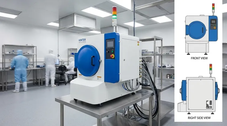
Visual Guide

Related Products
- RF PECVD System Radio Frequency Plasma-Enhanced Chemical Vapor Deposition RF PECVD
- Chemical Vapor Deposition CVD Equipment System Chamber Slide PECVD Tube Furnace with Liquid Gasifier PECVD Machine
- Tungsten Evaporation Boat for Thin Film Deposition
- CVD Diamond for Thermal Management Applications
- Customer Made Versatile CVD Tube Furnace Chemical Vapor Deposition Chamber System Equipment
People Also Ask
- What is an example of PECVD? RF-PECVD for High-Quality Thin Film Deposition
- How does plasma enhance CVD? Unlock Low-Temperature, High-Quality Film Deposition
- What is plasma enhanced chemical vapour deposition PECVD used for? Enable Low-Temp Thin Films for Electronics & Solar
- What is plasma chemical vapor deposition? A Low-Temperature Thin Film Coating Solution
- Why is a Matching Network Indispensable in RF-PECVD for Siloxane Films? Ensure Stable Plasma and Uniform Deposition


