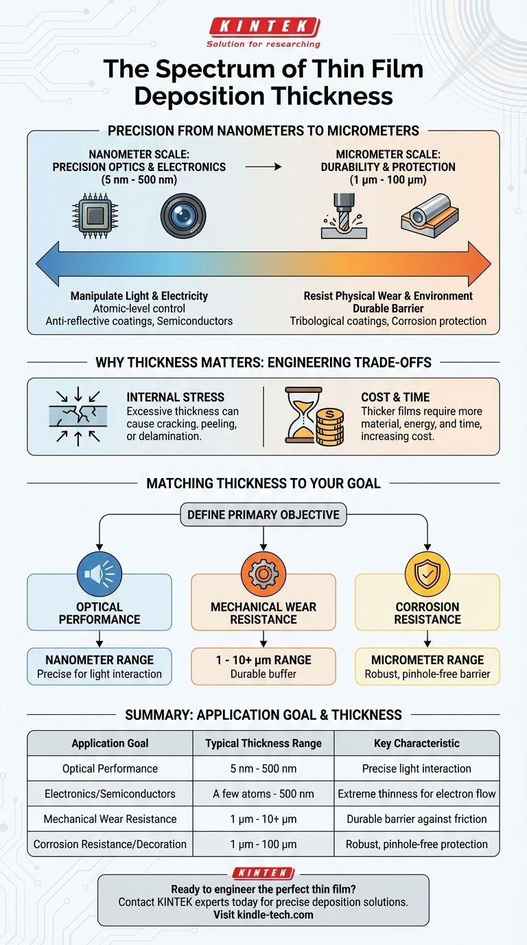
In thin film deposition, the thickness of a film is not a single value but a vast range, stretching from just a few nanometers (a handful of atoms) up to approximately 100 micrometers. This immense scale allows the technology to serve a wide array of highly specific industrial and scientific applications.
The central principle to understand is that a film's thickness is dictated entirely by its intended function. There is no "standard" thickness; instead, each layer is engineered to the precise dimension required to achieve a specific optical, mechanical, or electrical property.
Why Thickness is Application-Driven
The required thickness of a deposited film is a direct consequence of the physical problem it is designed to solve. A coating meant to manipulate light operates on a completely different scale than one designed to resist physical wear.
The Nanometer Scale: Precision Optics and Electronics
For applications involving the manipulation of light or electricity, control at the atomic level is critical.
Films in this range, often between 5 nm and 500 nm, are designed to interact with specific wavelengths of light. Anti-reflective coatings on eyeglasses or camera lenses, for example, must have a thickness that is a precise fraction of the light's wavelength to cause destructive interference and cancel out reflections.
In semiconductor manufacturing, layers of material can be just a few atoms thick. This extreme thinness is necessary to control the flow of electrons and create the complex transistor structures that power modern electronics.
The Micrometer Scale: Durability and Protection
When the primary goal is to protect a surface from physical harm, more material is required.
Coatings for tribological applications—such as reducing friction and wear on cutting tools or engine components—are typically in the 1 to 10 micrometer range. This thickness provides a durable barrier of hard material that can withstand significant mechanical stress and abrasion over time.
Similarly, decorative or corrosion-resistant coatings often fall into the micrometer range to ensure they are robust enough to resist scratches and environmental damage while providing a uniform appearance.
Understanding the Trade-offs of Thickness
Simply depositing a thicker film is not always a better solution. The process involves critical engineering trade-offs that limit the practical thickness for any given material and application.
The Problem of Internal Stress
As a film gets thicker during deposition, internal stresses build up within the material. If this stress becomes too high, it can exceed the adhesive force holding the film to the substrate.
This can cause the coating to crack, peel, or delaminate entirely, resulting in a complete failure of the part. Managing this internal stress is a primary challenge in developing thick protective coatings.
The Impact of Cost and Time
Deposition processes take time and consume source material and energy. As a result, a thicker film is almost always more expensive and time-consuming to produce.
Engineers must therefore find the minimum thickness required to achieve the desired performance, balancing functionality against manufacturing cost and throughput. A film should only be as thick as it absolutely needs to be.
Matching Thickness to Your Goal
To determine the right thickness, you must first define your primary objective. The functional requirement is the most important factor in the entire engineering decision.
- If your primary focus is optical performance: Your film thickness will be in the nanometer range, precisely calculated to interact with specific wavelengths of light.
- If your primary focus is mechanical wear resistance: You will be working in the single to low double-digit micrometer range to provide a sufficient buffer of durable material.
- If your primary focus is corrosion resistance: Thickness will likely be in the micrometer range to ensure a complete, pinhole-free barrier against the environment.
Ultimately, the right film thickness is a precise engineering decision, balancing the functional requirements of the application against the physical and economic limitations of the deposition process.
Summary Table:
| Application Goal | Typical Thickness Range | Key Characteristic |
|---|---|---|
| Optical Performance | 5 nm - 500 nm | Precise control for light interaction (e.g., anti-reflective coatings) |
| Electronics/Semiconductors | A few atoms - 500 nm | Extreme thinness for electron flow control |
| Mechanical Wear Resistance | 1 μm - 10+ μm | Durable barrier against friction and abrasion |
| Corrosion Resistance/Decoration | 1 μm - 100 μm | Robust, pinhole-free barrier for protection and appearance |
Ready to engineer the perfect thin film for your application?
At KINTEK, we specialize in providing the lab equipment and consumables needed to achieve precise, reliable film deposition. Whether your project requires nanometer precision for semiconductors or micrometer-thick durable coatings, our solutions help you balance performance with cost-effectiveness.
Contact our experts today to discuss your specific requirements and discover how KINTEK can support your laboratory's thin film innovation.
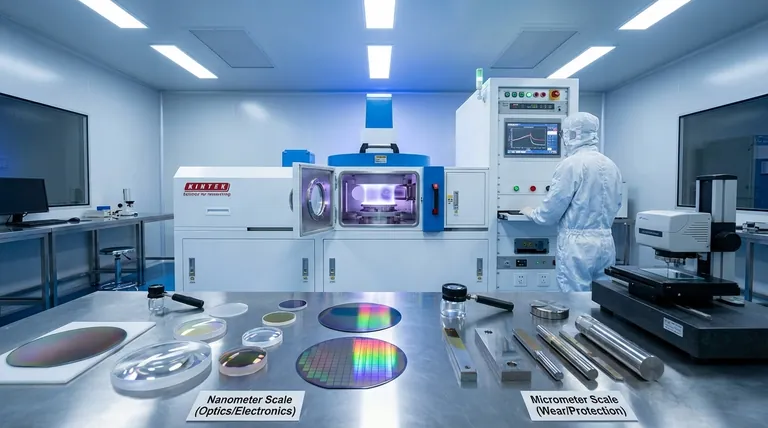
Visual Guide
Related Products
- Aluminized Ceramic Evaporation Boat for Thin Film Deposition
- Tungsten Evaporation Boat for Thin Film Deposition
- Hemispherical Bottom Tungsten Molybdenum Evaporation Boat
- Electron Beam Evaporation Coating Oxygen-Free Copper Crucible and Evaporation Boat
- Custom CVD Diamond Coating for Lab Applications
People Also Ask
- What is the source of evaporation for thin film? Choosing Between Thermal and E-Beam Methods
- What are thin films deposited by evaporation? A Guide to High-Purity Coating
- What are the applications of thin films deposition? Unlock New Possibilities for Your Materials
- What is the chemical method for thin film deposition? Build Films from the Molecular Level Up
- What is the widely used boat made of in thermal evaporation? Choosing the Right Material for High-Purity Deposition


