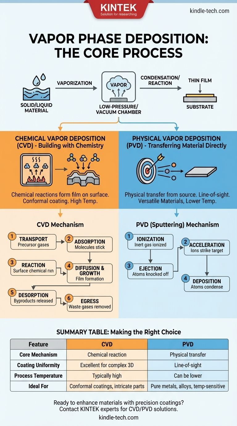
At its core, vapor phase deposition is a family of advanced manufacturing processes used to apply very thin, high-performance coatings onto a surface, known as a substrate. These processes all work by converting a solid or liquid coating material into a vapor, transporting it through a low-pressure or vacuum environment, and then allowing it to condense or react on the substrate's surface to form a solid film. The two primary categories of this technology are Chemical Vapor Deposition (CVD) and Physical Vapor Deposition (PVD).
The fundamental distinction between vapor deposition methods lies in the mechanism. Chemical Vapor Deposition (CVD) uses chemical reactions on the substrate's surface to form the film, while Physical Vapor Deposition (PVD) physically transports material from a source to the substrate without initiating a new chemical reaction.
The Two Pillars of Vapor Deposition
To understand the field, you must first grasp the critical difference between its two main branches: chemical and physical deposition.
Chemical Vapor Deposition (CVD): Building with Chemistry
In CVD, the substrate is placed inside a reaction chamber and heated. Volatile precursor gases, which contain the atoms required for the final film, are then introduced into the chamber.
The high temperature causes these gases to react or decompose on the substrate's surface, forming a new, solid material that bonds directly to it. This process effectively "grows" a film layer by layer through a controlled chemical reaction.
Because the precursor is a gas, it can flow into and coat all exposed areas of a part, making CVD excellent for creating uniform coatings on complex, three-dimensional shapes.
Physical Vapor Deposition (PVD): Transferring Material Directly
In PVD, the coating material starts as a solid source, often called a "target." In a vacuum, this target is bombarded with energy—for example, by a high-energy plasma in a process called sputtering, or by heating it until it evaporates.
This process ejects atoms or molecules from the target, which then travel in a straight line through the vacuum and condense onto the substrate.
Unlike CVD, no chemical reaction is intended to occur on the substrate. The process is a physical transfer, much like spraying a microscopic layer of atoms from a source to a target.
Deconstructing the Deposition Process
While the high-level concepts are distinct, the detailed mechanisms reveal the underlying science and engineering control required for each method.
The CVD Mechanism in Detail
The CVD process is a sequence of carefully controlled physicochemical events:
- Transport: Precursor gases are delivered into the reaction chamber.
- Adsorption: The gas molecules stick to the heated surface of the substrate.
- Reaction: The adsorbed molecules undergo a chemical reaction on the surface, often catalyzed by the heat.
- Diffusion & Growth: The newly formed film atoms diffuse across the surface to find stable nucleation sites and build the film structure.
- Desorption: Gaseous byproducts from the reaction are released from the surface.
- Egress: These waste gases are transported out of the reaction chamber.
A Common PVD Mechanism: Sputtering
Sputtering is a dominant PVD technique that uses plasma to generate vapor:
- Ionization: An inert gas, typically argon, is introduced into the vacuum chamber and ionized to create a plasma.
- Acceleration: The positive argon ions are accelerated by an electric field, causing them to strike the solid target material with high energy.
- Ejection: The impact of these ions physically knocks atoms off the target material.
- Deposition: These ejected atoms travel through the vacuum and condense on the cooler substrate, forming the thin film.
Understanding the Trade-offs
Neither process is universally superior; the choice depends entirely on the material, the substrate, and the desired outcome. Understanding their limitations is critical for making an informed decision.
CVD: Conformality vs. Complexity
CVD's greatest strength is its conformality—the ability of the gas to uniformly coat intricate shapes and internal surfaces.
However, it often requires very high temperatures, which can damage heat-sensitive substrates. The precursor chemicals can also be hazardous, and controlling the precise chemical reactions adds a layer of process complexity.
PVD: Line-of-Sight vs. Versatility
PVD is often a "line-of-sight" process. Since the vaporized atoms travel in a straight line, it is difficult to coat the interior of complex geometries or the "back side" of a part without complex rotation and fixturing.
Its advantage lies in its versatility and purity. PVD can deposit a vast range of materials, including pure metals, alloys, and ceramics with extremely high melting points, often at lower process temperatures than CVD.
Equipment and Material Limitations
All deposition processes have practical constraints. For example, in certain CVD methods like Hot Filament CVD (HFCVD), the heated filament used to activate the gases can degrade and form carbides over time. This mechanical deterioration eventually leads to failure and represents a consumable part of the process.
Making the Right Choice for Your Application
Selecting the correct process requires aligning the technique's strengths with your primary engineering goal.
- If your primary focus is coating complex 3D shapes uniformly: CVD is almost always the superior choice due to its non-line-of-sight nature and excellent conformality.
- If your primary focus is depositing pure metals, refractory materials, or alloys with high melting points: PVD excels at physically transferring these materials without the complexities of precursor chemistry.
- If your primary focus is processing temperature-sensitive substrates: PVD often provides lower-temperature options compared to many high-temperature CVD processes.
Understanding the fundamental mechanism—chemical reaction versus physical transfer—is the key to selecting the optimal vapor deposition technique for any engineering challenge.
Summary Table:
| Feature | Chemical Vapor Deposition (CVD) | Physical Vapor Deposition (PVD) |
|---|---|---|
| Core Mechanism | Chemical reaction on substrate surface | Physical transfer of material |
| Coating Uniformity | Excellent for complex 3D shapes | Line-of-sight (requires fixturing) |
| Process Temperature | Typically high | Can be lower |
| Ideal For | Conformal coatings, intricate parts | Pure metals, alloys, temperature-sensitive substrates |
Ready to enhance your materials with precision thin-film coatings?
Whether your project requires the uniform coverage of Chemical Vapor Deposition (CVD) or the versatile material options of Physical Vapor Deposition (PVD), KINTEK has the expertise and equipment to meet your laboratory's needs. Our specialized lab equipment and consumables are designed to support advanced coating applications, ensuring high performance and reliability.
Contact our experts today to discuss how our vapor phase deposition solutions can bring value to your research and development.
Visual Guide
Related Products
- Chemical Vapor Deposition CVD Equipment System Chamber Slide PECVD Tube Furnace with Liquid Gasifier PECVD Machine
- 915MHz MPCVD Diamond Machine Microwave Plasma Chemical Vapor Deposition System Reactor
- RF PECVD System Radio Frequency Plasma-Enhanced Chemical Vapor Deposition RF PECVD
- Microwave Plasma Chemical Vapor Deposition MPCVD Machine System Reactor for Lab and Diamond Growth
- HFCVD Machine System Equipment for Drawing Die Nano-Diamond Coating
People Also Ask
- What are the core advantages of PE-CVD in OLED encapsulation? Protect Sensitive Layers with Low-Temp Film Deposition
- What is plasma enhanced chemical vapor deposition PECVD equipment? A Guide to Low-Temperature Thin Film Deposition
- What is the chemical vapor deposition growth process? Build Superior Thin Films from the Atom Up
- What are the processes of vapor phase deposition? Understand CVD vs. PVD for Superior Thin Films
- How expensive is chemical vapor deposition? Understanding the True Cost of High-Performance Coating


