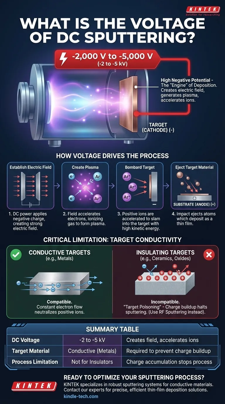
In DC sputtering, the applied voltage is a high negative potential typically ranging from -2,000 to -5,000 volts (-2 to -5 kV). This voltage is applied directly to the target material, which acts as the cathode. This specific electrical condition is the fundamental driver of the entire deposition process.
The high DC voltage isn't just a setting; it's the engine of the sputtering process. Its primary purpose is to create a strong electric field that generates a plasma and then aggressively accelerates positive ions into the target, physically blasting atoms loose for deposition.
How Voltage Drives the Sputtering Process
To understand DC sputtering, you must understand the precise role this high voltage plays at each step. It orchestrates a chain reaction inside the vacuum chamber.
Establishing the Electric Field
The process begins when the DC power supply applies the negative -2 to -5 kV charge to the target material (the cathode). The chamber walls or a dedicated electrode act as the anode (the positive side), creating a powerful electric field between them.
Creating the Plasma
Within the low-pressure gas environment (typically Argon), stray free electrons are accelerated by this intense electric field. As they gain speed and energy, they collide with neutral gas atoms, stripping them of their own electrons.
This event creates two new particles: another free electron and a positively charged gas ion. This cascade of collisions quickly ignites and sustains a visible plasma, which is simply a cloud of these charged ions and free electrons.
Bombarding the Target
The newly created positive ions are now strongly attracted to the highly negative target. The electric field accelerates these ions, causing them to slam into the target's surface with significant kinetic energy.
Ejecting the Target Material
This high-energy ion bombardment is a physical, not chemical, process. The impact has enough force to knock atoms or molecules loose from the target material. These "sputtered" atoms then travel through the chamber and deposit as a thin film onto the substrate.
The Critical Limitation of DC Voltage
The use of a direct current (DC) voltage is both the system's strength and its primary weakness. It defines which materials you can and cannot deposit.
The Conductive Target Requirement
DC sputtering is only effective for electrically conductive target materials, such as pure metals. A constant flow of electrons through the target is necessary to maintain the negative charge and neutralize the positive ions that are constantly striking it.
The Problem of Insulating Materials
If you attempt to use a non-conductive (insulating) target, a phenomenon known as "target poisoning" occurs. The positive charge from the bombarding gas ions accumulates on the target's surface because the material cannot conduct it away.
This buildup of positive charge effectively neutralizes the negative voltage, shielding the target from further ion bombardment. The plasma may remain lit, but the sputtering process grinds to a halt.
Making the Right Choice for Your Goal
The voltage type is the most critical factor in choosing a sputtering system. Your decision must be based on the material you intend to deposit.
- If your primary focus is depositing metals or other conductive materials: DC sputtering is the most efficient and cost-effective method due to its high deposition rates and simpler power supply.
- If your primary focus is depositing insulators (like ceramics or oxides): DC sputtering is fundamentally incompatible with your goal, and you must use a technique like RF (Radio Frequency) sputtering to prevent charge buildup.
Ultimately, understanding the role of voltage is the key to selecting the right sputtering technique for your material.
Summary Table:
| Parameter | Typical Range | Purpose |
|---|---|---|
| DC Voltage | -2,000 to -5,000 V (-2 to -5 kV) | Creates electric field, accelerates ions to sputter target material |
| Target Material | Electrically conductive (e.g., metals) | Required for DC sputtering to prevent charge buildup |
| Process Limitation | Not suitable for insulating materials (ceramics, oxides) | Charge accumulation halts sputtering; RF sputtering is required instead |
Ready to Optimize Your Sputtering Process?
DC sputtering is ideal for high-rate deposition of conductive materials, but selecting the right equipment is crucial for your specific application. KINTEK specializes in lab equipment and consumables, offering robust sputtering systems tailored to your research and production needs.
Let us help you achieve precise, efficient thin-film deposition. Contact our experts today to discuss your project requirements and discover how KINTEK's solutions can enhance your laboratory's capabilities.
Visual Guide
Related Products
- Laboratory Scientific Electric Heating Blast Drying Oven
- Single Punch Electric Tablet Press Machine TDP Tablet Punching Machine
People Also Ask
- What role does a precision laboratory drying oven play in the synthesis of GO-PANI nanocomposites? Protect Material Integrity
- What is the function of a laboratory drying oven in Zr2.5Nb alloy pretreatment? Ensure Precise Corrosion Test Results
- What is the role of a laboratory blast drying oven in the production of solid-state corrosion inhibitors? - KINTEK
- What is the role of a laboratory drying oven in cellulose citrate production? Ensure Material Stability & Purity
- Why is a laboratory drying oven essential for biomass liquefaction? Ensure Accurate Conversion Rate Calculations

