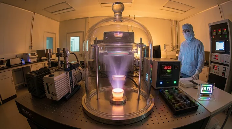
In simple terms, organic thermal evaporation is a manufacturing technique used to create ultra-thin films from organic compounds. It operates under a high vacuum by gently heating an organic source material until it turns into a vapor, which then condenses onto a cooler surface, known as a substrate, to form a precise and uniform layer. This method is the cornerstone for building modern electronic devices like OLED screens.
The core challenge in working with organic materials is their fragility; they are easily destroyed by high temperatures or energy. Thermal evaporation is the preferred method because it is gentle enough to turn these complex molecules into a vapor without breaking them apart, preserving the chemical integrity required for functional electronic devices.
How Organic Thermal Evaporation Works
The process, a specific type of physical vapor deposition (PVD), is elegant in its simplicity but requires extreme precision. It is fundamentally different from evaporating simple metals due to the delicate nature of organic molecules.
The High-Vacuum Environment
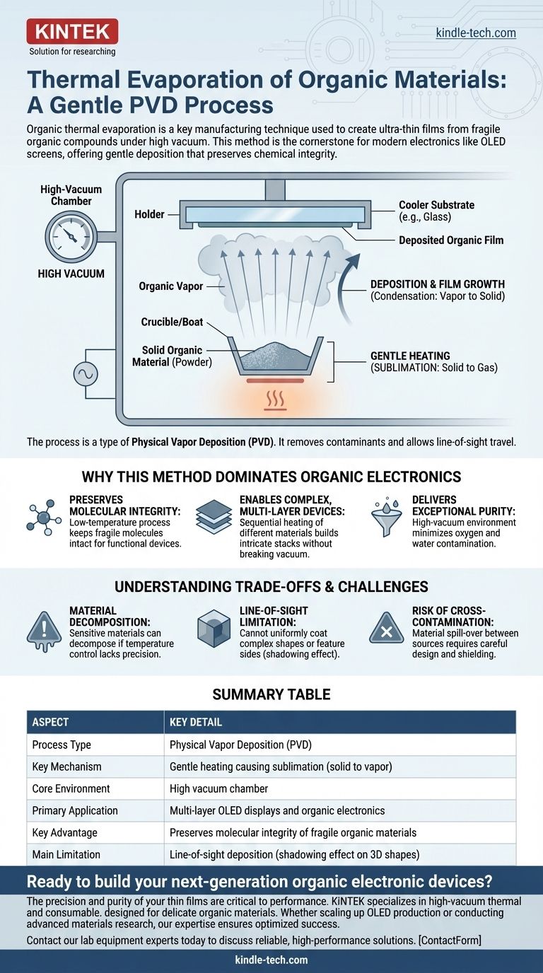
Everything happens inside a chamber pumped down to a high vacuum. This serves two critical purposes: it removes air molecules that could react with and contaminate the organic vapor, and it allows the vaporized molecules to travel in a straight line to the substrate without colliding with anything.
The Gentle Heating Process
The solid organic material, often a fine powder, is placed in a container called a crucible or "boat." This crucible is then gently heated, typically using electrical resistance.
Unlike metals that melt and then boil, most organic materials for electronics undergo sublimation—they transition directly from a solid to a gas. This requires significantly lower temperatures, which is key to preventing the complex organic molecules from decomposing.
Deposition and Film Growth
The gaseous organic molecules travel outward from the source. They eventually strike a much cooler substrate (like the glass for a display screen) positioned above the source.
Upon contact, the molecules instantly cool and condense back into a solid state, forming a highly uniform, ultra-thin film on the substrate's surface. By precisely controlling the source temperature and deposition time, engineers can dictate the exact thickness of the film, often with nanometer-level accuracy.
Why This Method Dominates Organic Electronics
Other deposition techniques, like sputtering, are far too aggressive for organic materials. Thermal evaporation became the industry standard for specific, critical reasons.
It Preserves Molecular Integrity
This is the most important advantage. The functionality of an organic electronic device, such as an OLED or an organic solar cell, depends entirely on the precise structure of its organic molecules. The low-temperature, low-energy nature of thermal evaporation deposits these molecules intact.
It Enables Complex, Multi-Layer Devices
Modern OLED displays are not made of a single film but a stack of many different organic layers. Each layer performs a specific function (e.g., injecting, transporting, or emitting light).
Thermal evaporation systems can house multiple crucibles, each containing a different organic material. By heating them in sequence, manufacturers can build these intricate multi-layer structures without ever breaking the vacuum, ensuring pristine interfaces between layers.
It Delivers Exceptional Purity
The high-vacuum environment is essential for creating high-performance devices. It minimizes the risk of oxygen or water molecules—major sources of contamination—getting trapped in the thin film, which would degrade device performance and shorten its lifespan.
Understanding the Trade-offs and Challenges
While it is the dominant technique, organic thermal evaporation is not without its operational complexities.
Potential for Material Decomposition
Even with low temperatures, some organic materials are exceptionally sensitive and can decompose if the temperature is not controlled with extreme precision. A stable deposition rate is critical for consistent device manufacturing.
Line-of-Sight Limitation
The organic vapor travels in a straight line from the source to the substrate. This means the process cannot uniformly coat complex, three-dimensional shapes or the sides of features on a substrate. This is known as the "shadowing effect."
Risk of Cross-Contamination
In systems with multiple sources for creating layer stacks, there is a risk that material from one source can "spill over" and contaminate an adjacent source or layer. This requires careful system design and shielding to prevent.
Making the Right Choice for Your Goal
Understanding the nuance of this technique is key to applying it correctly for your specific objective.
- If your primary focus is creating high-performance OLEDs or organic solar cells: You must use a multi-source thermal evaporation system to build the required complex, high-purity layer stacks.
- If your primary focus is fundamental research on new materials: A simpler, single-source system is often sufficient to test the deposition properties and viability of new organic compounds.
- If your goal is to deposit robust materials like metal contacts: You will still use thermal evaporation, but the process will require much higher temperatures and different source materials compared to the delicate process for organics.
Mastering this gentle deposition technique is fundamental to fabricating the advanced organic electronics that define our modern world.
Summary Table:
| Aspect | Key Detail |
|---|---|
| Process Type | Physical Vapor Deposition (PVD) |
| Key Mechanism | Gentle heating causing sublimation (solid to vapor) |
| Core Environment | High vacuum chamber |
| Primary Application | Multi-layer OLED displays and organic electronics |
| Key Advantage | Preserves molecular integrity of fragile organic materials |
| Main Limitation | Line-of-sight deposition (shadowing effect on 3D shapes) |
Ready to build your next-generation organic electronic devices? The precision and purity of your thin films are critical to performance. KINTEK specializes in high-vacuum thermal evaporation systems and consumables designed specifically for the delicate needs of organic materials. Whether you are scaling up OLED production or conducting advanced materials research, our expertise ensures your process is optimized for success. Contact our lab equipment experts today to discuss how we can support your specific application with reliable, high-performance solutions.
Visual Guide
Related Products
- Molybdenum Tungsten Tantalum Evaporation Boat for High Temperature Applications
- Aluminized Ceramic Evaporation Boat for Thin Film Deposition
- Evaporation Boat for Organic Matter
- Multi Heating Zones CVD Tube Furnace Machine Chemical Vapor Deposition Chamber System Equipment
- Chemical Vapor Deposition CVD Equipment System Chamber Slide PECVD Tube Furnace with Liquid Gasifier PECVD Machine
People Also Ask
- What are the sources of thermal evaporation? A Guide to Resistive vs. E-Beam Heating
- What is the source of evaporation for thin film? Choosing Between Thermal and E-Beam Methods
- How does a molybdenum evaporation source function in H2S for MoS2 synthesis? Master Reactive Film Deposition
- What are thermal evaporation sources? Key Types and How to Choose the Right One
- Is thermal evaporation used to deposit a thin metal film? A Guide to This Foundational PVD Technique