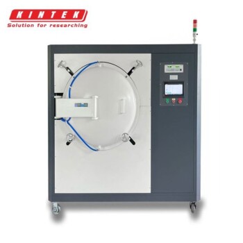
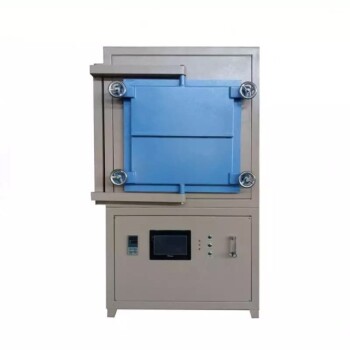
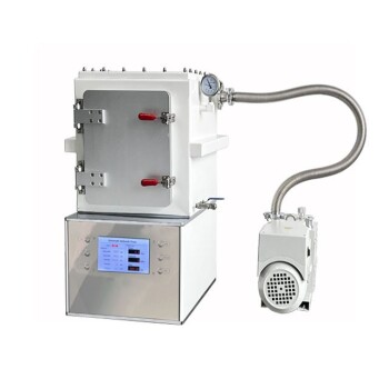
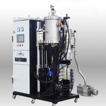
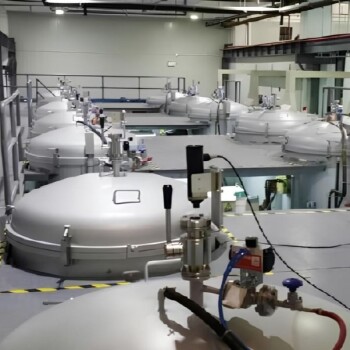
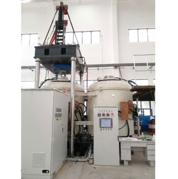
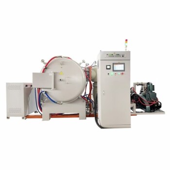
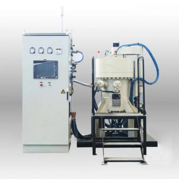
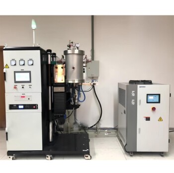
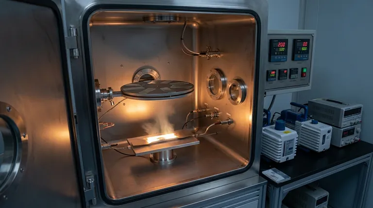
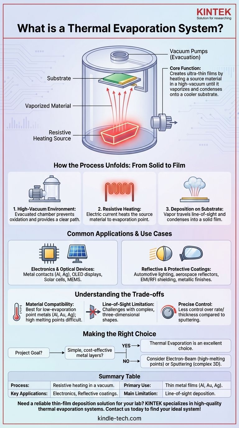
At its core, a thermal evaporation system is a machine that creates exceptionally thin films of material onto a surface. It works by heating a source material inside a high-vacuum chamber until it vaporizes, allowing the resulting vapor to travel and condense onto a cooler substrate, forming a uniform coating. This technique, also known as resistive evaporation, is a fundamental process in creating many modern electronic and optical components.
The central concept is straightforward: use electrical resistance to generate heat, turn a solid material into a gas in a vacuum, and let that gas re-solidify as a precise, thin layer on a target object. This elegant simplicity makes it a cornerstone of thin-film deposition technology.
How the Process Unfolds: From Solid to Film
The entire process relies on controlling a physical transformation within a highly controlled environment. Each step is critical to achieving a high-quality, uniform film.
The Critical Role of the Vacuum
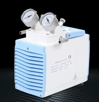
A thermal evaporator's primary component is a vacuum chamber. This chamber is evacuated by powerful pumps to remove air and other gas molecules.
This high-vacuum environment is essential for two reasons. First, it prevents the hot source material from reacting with gases like oxygen. Second, it provides a clear, unimpeded path for the vaporized atoms to travel from the source to the substrate.
Heating the Source Material
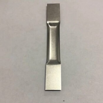
Inside the chamber, the material to be deposited (the source material) is placed in a small container, often called a "boat" or "basket." This boat is made of a material that can withstand extreme temperatures and has high electrical resistance.
An electric current is passed through the boat, causing it to heat up intensely due to its resistance. This heat is transferred to the source material, raising its temperature until it reaches its evaporation point and turns into a vapor.
Deposition onto the Substrate
Positioned above the source is the object to be coated, known as the substrate. This substrate is held in place by a fixture.
As the source material vaporizes, its atoms travel in a straight line-of-sight path through the vacuum. When these atoms hit the cooler surface of the substrate, they condense back into a solid state, gradually building up to form a thin, solid film.
Common Applications and Use Cases
Thermal evaporation is valued for its relative simplicity and effectiveness, particularly for depositing single metals with high purity.
Electronics and Optical Devices
This method is a workhorse in the production of electronic components. It is commonly used for depositing metal electrical contacts, such as aluminum or silver, on semiconductors and other devices.
It also plays a key role in manufacturing OLED displays, solar cells, and microelectromechanical systems (MEMS), where precise layers of conductive or reflective material are required.
Reflective and Protective Coatings
The ability to create highly reflective metal layers makes thermal evaporation ideal for manufacturing light reflectors. These are used in automotive lighting, medical equipment, and aerospace components.
It is also used for applying EMI/RFI shielding on electronic housings and for creating decorative metallic finishes on items like cosmetic packaging and sporting goods.
Understanding the Trade-offs
While powerful, thermal evaporation is not the solution for every thin-film challenge. Understanding its limitations is key to using it effectively.
Material Compatibility
The process works best for materials with relatively low evaporation points, such as aluminum, gold, silver, and chromium. Materials with extremely high melting points or complex alloys can be difficult or impossible to deposit using simple resistive heating.
Line-of-Sight Limitation
Because the vaporized atoms travel in straight lines, the process can only coat surfaces that have a direct line of sight to the source. This makes it challenging to achieve uniform coatings on complex, three-dimensional shapes with undercuts or hidden surfaces.
Precise Control Challenges
While effective, precisely controlling the deposition rate and film thickness can be more difficult with thermal evaporation compared to more advanced techniques like sputtering or electron-beam evaporation.
Making the Right Choice for Your Goal
Selecting a deposition method depends entirely on the material, substrate, and desired outcome of your project.
- If your primary focus is creating simple, cost-effective metal layers: Thermal evaporation is an excellent and widely used choice, especially for electrical contacts or basic reflective coatings.
- If your primary focus is depositing materials with very high melting points or complex alloys: You should consider more advanced methods like electron-beam evaporation, which can achieve much higher temperatures.
- If your primary focus is uniformly coating a complex 3D object: A non-line-of-sight process like sputtering or chemical vapor deposition would be a more suitable technology.
Ultimately, thermal evaporation provides a direct and reliable path for transforming a solid material into a high-performance thin film.
Summary Table:
| Aspect | Key Detail |
|---|---|
| Process | Resistive heating in a vacuum to vaporize a source material. |
| Primary Use | Depositing thin films of metals like aluminum, gold, and silver. |
| Key Applications | Electronic contacts, OLEDs, solar cells, reflective coatings. |
| Main Limitation | Line-of-sight deposition; challenges with complex 3D shapes. |
Need a reliable thin-film deposition solution for your lab?
KINTEK specializes in high-quality lab equipment, including thermal evaporation systems perfect for creating precise metal coatings for electronics, optics, and research. Our experts can help you select the right system to enhance your project's efficiency and performance.
Contact us today to discuss your specific application and discover the ideal thermal evaporation system for your laboratory needs.
Visual Guide
Related Products
- Molybdenum Tungsten Tantalum Evaporation Boat for High Temperature Applications
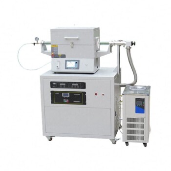
- Split Chamber CVD Tube Furnace with Vacuum Station Chemical Vapor Deposition System Equipment Machine
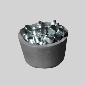
- Electron Beam Evaporation Coating Conductive Boron Nitride Crucible BN Crucible
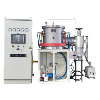
- 2200 ℃ Tungsten Vacuum Heat Treat and Sintering Furnace
- Vacuum Heat Treat Furnace with Ceramic Fiber Liner
People Also Ask
- What is vacuum thermal evaporation? A Guide to High-Purity Thin Film Deposition
- What is thermal effect via evaporation? A Simple Guide to Thin-Film Deposition
- What is the thermal evaporation technique? A Guide to Thin-Film Deposition for Your Lab
- What is thermal evaporation used to deposit? A Guide to Metals, Compounds, and Key Applications
- What are the drawbacks of thermal evaporation? Understanding the Limitations for High-Performance Applications
