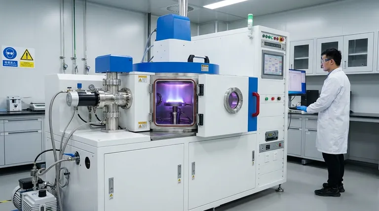
In essence, magnetron sputtering is a high-precision manufacturing process used to deposit exceptionally thin layers of material onto a surface. It functions like a microscopic sandblaster, using energized gas ions in a vacuum to knock atoms off a source material (the "target") and uniformly coat a second object (the "substrate"), creating a high-quality, dense thin film. This technique is a cornerstone of modern manufacturing for products like semiconductors, optical lenses, and medical implants.
The core value of magnetron sputtering isn't just coating a surface; it's a method for engineering materials at an atomic level. It provides the precise control needed to create the high-performance films that are essential for advanced electronics and optical devices.
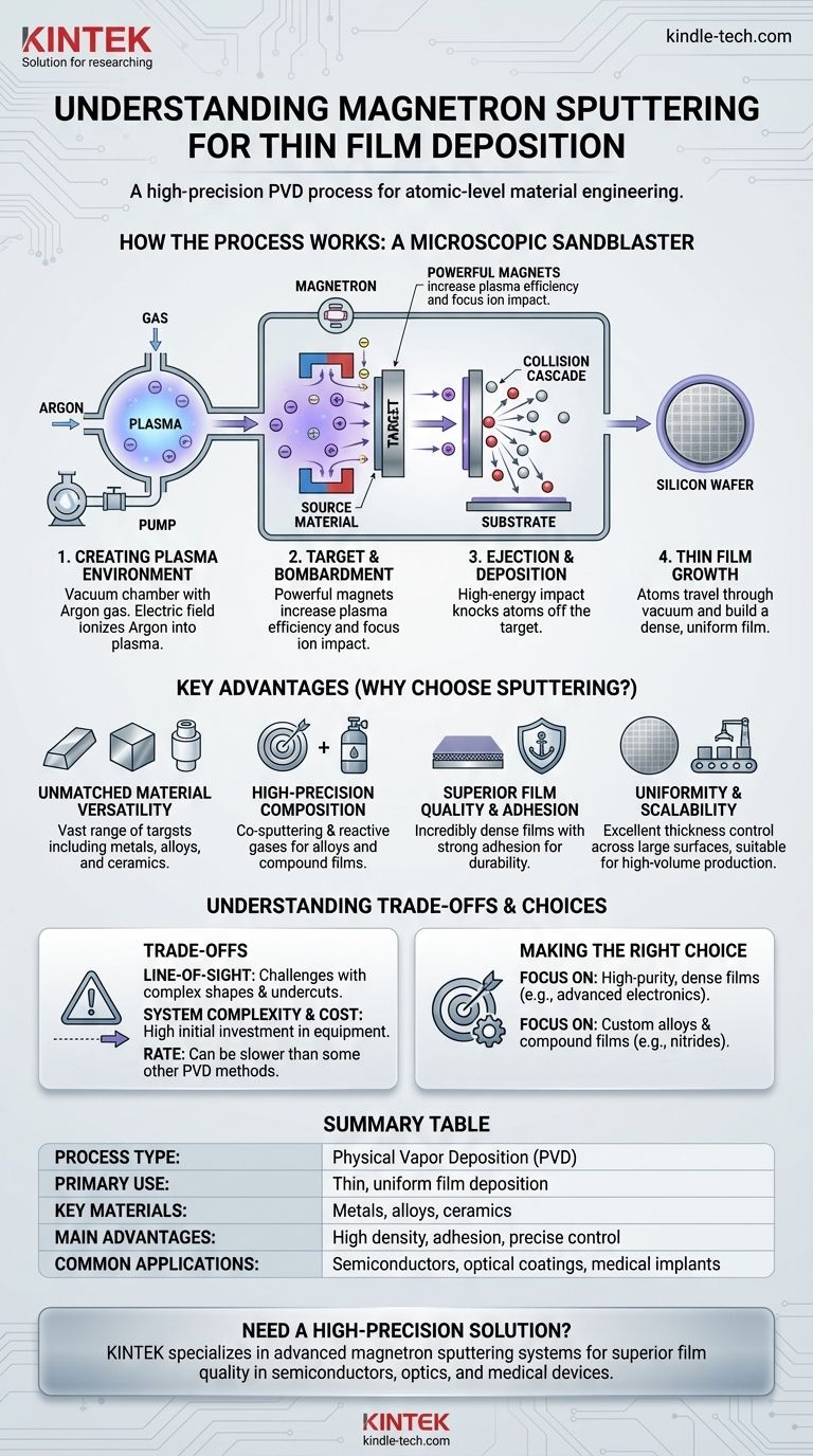
How the Sputtering Process Works
Magnetron sputtering is a form of physical vapor deposition (PVD), meaning it physically transfers material from a solid source to the substrate without a chemical reaction. The process unfolds within a controlled vacuum chamber.
Creating the Plasma Environment
First, a vacuum chamber is pumped down to remove air and other contaminants. A small amount of a noble gas, typically Argon, is then introduced into the chamber.
The Target and the Bombardment
A powerful electric field is applied, which energizes the Argon gas and strips electrons from the atoms, creating a glowing, ionized gas known as a plasma. The "magnetron" component uses powerful magnets behind the target to trap these electrons, dramatically increasing the efficiency of the plasma and focusing the ion bombardment onto the target material.
Ejection and Deposition
The positively charged gas ions from the plasma are accelerated into the negatively charged target surface. This high-energy impact physically knocks loose, or "sputters," atoms from the target material, creating a "collision cascade."
Thin Film Growth
These ejected target atoms travel through the vacuum chamber and land on the substrate (such as a silicon wafer or solar panel), gradually building a thin, dense, and highly uniform film one atomic layer at a time.
Key Advantages of Magnetron Sputtering
Engineers and scientists choose this method when the properties of the final film are critical. The control and quality it offers are its primary advantages.
Unmatched Material Versatility
A vast range of materials can be used as targets, including pure metals, complex alloys, and even ceramics. This allows for the deposition of almost any inorganic material.
High-Precision Composition
Multiple targets can be used simultaneously (co-sputtering) to create films of specific alloys with precise compositions. Furthermore, reactive gases like nitrogen or oxygen can be introduced to form compound films, such as nitrides and oxides, directly on the substrate.
Superior Film Quality and Adhesion
Sputtering produces films that are incredibly dense and adhere very strongly to the substrate. This is critical for the durability and performance of microprocessors, disk drives, and optical coatings.
Uniformity and Scalability
The process allows for exceptionally uniform film thickness across large surfaces, which is essential for mass-producing items like silicon wafers or CDs. The high deposition rates make it suitable for high-volume, efficient industrial production.
Understanding the Trade-offs
While powerful, magnetron sputtering is not the only method for creating thin films, and it's essential to understand its context.
A Line-of-Sight Process
As a physical deposition method, sputtering generally works in a "line of sight." Atoms travel in a relatively straight line from the target to the substrate, which can make it challenging to evenly coat complex, three-dimensional shapes with deep trenches or undercuts.
System Complexity and Cost
Magnetron sputtering systems are sophisticated pieces of equipment that require high vacuum, powerful electronics, and precise controls. This makes the initial investment significantly higher than simpler methods like chemical bath deposition or the sol-gel process.
Rate vs. Other Methods
While considered a high-rate deposition technique, it can be slower than other PVD methods like thermal evaporation for certain materials. The trade-off is that sputtering provides far greater control over the film's final structure and properties.
Making the Right Choice for Your Goal
Selecting a deposition method depends entirely on the requirements for the final product, balancing cost, quality, and material properties.
- If your primary focus is high-purity, dense films for advanced electronics or optics: Magnetron sputtering is the industry standard due to its unmatched control over film quality and uniformity.
- If your primary focus is creating custom alloys or specific compound films (like nitrides): The co-sputtering and reactive gas capabilities of this method make it the ideal choice.
- If your primary focus is a simple, low-cost coating where atomic-level precision is not required: Simpler techniques like chemical bath deposition may be more suitable and cost-effective.
Ultimately, magnetron sputtering is the enabling technology that provides the atomic-level control required to build the high-performance materials that power our modern world.
Summary Table:
| Key Aspect | Details |
|---|---|
| Process Type | Physical Vapor Deposition (PVD) |
| Primary Use | Depositing thin, uniform films on substrates |
| Key Materials | Metals, alloys, ceramics (via pure or reactive sputtering) |
| Main Advantages | High film density, strong adhesion, precise composition control, scalability |
| Common Applications | Semiconductors, optical coatings, medical implants, solar panels |
Need a high-precision thin film deposition solution for your lab? KINTEK specializes in advanced lab equipment, including magnetron sputtering systems, to help you achieve superior film quality for semiconductors, optics, and medical devices. Our expertise ensures you get the right setup for precise, uniform coatings tailored to your research or production needs. Contact us today to discuss how we can enhance your laboratory capabilities!
Visual Guide
Related Products
- Spark Plasma Sintering Furnace SPS Furnace
- RF PECVD System Radio Frequency Plasma-Enhanced Chemical Vapor Deposition RF PECVD
People Also Ask
- Why are Spark Plasma Sintering (SPS) furnaces or hot presses utilized in the preparation of Li3PS4 solid electrolytes?
- What are the advantages of CAMI/SPS for W-Cu composite preparation? Reduce cycles from hours to seconds.
- What is the process fundamentals of spark plasma sintering? Achieve Rapid, High-Density Material Consolidation
- What are the fundamentals of spark plasma sintering process? Unlock Rapid, High-Performance Material Consolidation
- What technical advantages does a Spark Plasma Sintering (SPS) furnace offer for LZP ceramics? Enhance Ionic Conductivity

