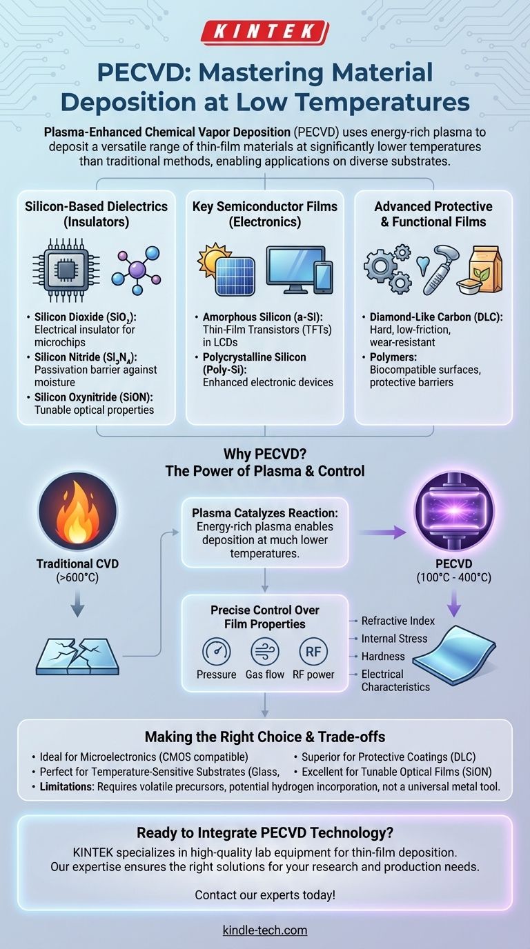
In short, Plasma-Enhanced Chemical Vapor Deposition (PECVD) is a highly versatile process used to deposit a wide range of thin-film materials. The most common materials include silicon-based compounds like silicon nitride (Si₃N₄) and **silicon dioxide (SiO₂) **, semiconductor films like amorphous silicon (a-Si), and hard protective coatings such as diamond-like carbon (DLC). It can also deposit certain metals and polymers.
The true value of PECVD is not just the variety of materials it can deposit, but its ability to do so at low temperatures. This use of an energy-rich plasma, rather than high heat, allows for the creation of high-quality functional films on a vast array of substrates, including those that cannot withstand high temperatures.
Understanding the Core Material Groups
PECVD's versatility stems from its ability to form different types of films by selecting specific precursor gases. These deposited materials can be broadly categorized by their function and composition.
The Workhorses: Silicon-Based Dielectrics
The most widespread use of PECVD is in microelectronics for depositing insulating, or dielectric, films.
- Silicon Dioxide (SiO₂): An excellent electrical insulator, used to isolate conductive layers within a microchip. It is typically formed using precursor gases like silane (SiH₄) and nitrous oxide (N₂O).
- Silicon Nitride (Si₃N₄): A robust insulator that also serves as a superior barrier against moisture and ion diffusion. It is often used as a final passivation layer to protect the chip from the environment. It is formed from gases like silane (SiH₄) and ammonia (NH₃).
- Silicon Oxynitride (SiON): A compound that combines the properties of both oxide and nitride. By adjusting the gas mixture, its properties, such as refractive index, can be precisely tuned for optical applications.
Key Semiconductor Films
PECVD is also critical for depositing silicon films that have semiconductor properties, which are foundational for solar cells and display technology.
- Amorphous Silicon (a-Si): A non-crystalline form of silicon that is essential for manufacturing thin-film transistors (TFTs) used in LCD screens.
- Polycrystalline Silicon (Poly-Si): A form of silicon made of many small crystals. It has better electronic properties than a-Si and is used in various electronic devices.
Advanced Protective and Functional Films
Beyond silicon, PECVD enables the deposition of specialized materials for mechanical and biomedical applications.
- Diamond-Like Carbon (DLC): An extremely hard, low-friction material. It is used as a protective coating on tools, medical implants, and engine parts to dramatically reduce wear and friction.
- Polymers: PECVD can deposit thin polymer layers, including hydrocarbons and silicones. These films are used as protective barriers in food packaging and for creating biocompatible surfaces on medical devices.
Why PECVD is a Versatile Deposition Method
The "what" of PECVD (the materials) is directly enabled by the "how" (the process). The key is its use of plasma instead of relying solely on thermal energy.
The Power of Plasma
In traditional Chemical Vapor Deposition (CVD), very high temperatures (often >600°C) are needed to break down precursor gases and initiate the chemical reaction.
The plasma in PECVD acts as a catalyst. It energizes the gas molecules, allowing them to react and deposit onto the substrate at much lower temperatures, typically between 100°C and 400°C.
Control Over Film Properties
This low-temperature process gives engineers immense control. By precisely adjusting process parameters like gas flow rates, pressure, and radio-frequency (RF) power, you can fine-tune the final properties of the film.
This control allows for tailoring a material's refractive index, internal stress, hardness, and electrical characteristics to meet the specific demands of the application.
Understanding the Trade-offs
While powerful, PECVD is not a universal solution. Understanding its limitations is key to using it effectively.
The Need for Volatile Precursors
The fundamental requirement for PECVD is the availability of precursor materials that are gases or can be easily vaporized. The process is limited to materials for which suitable, high-purity precursor gases exist.
Potential for Impurities
Because the process often uses hydrogen-containing precursors (like silane, SiH₄), it is possible for hydrogen to become incorporated into the deposited film. This can sometimes affect the film's electrical or mechanical properties.
Not a Universal Metal Deposition Tool
While some metals can be deposited with PECVD, other techniques like Physical Vapor Deposition (PVD) are often more practical for a wider range of metallic films, especially complex alloys.
Making the Right Choice for Your Goal
Your choice of deposition technology should always be driven by your end goal. PECVD is a superior choice in several key scenarios.
- If your primary focus is microelectronics: PECVD is the industry standard for depositing high-quality insulating (SiO₂, Si₃N₄) and semiconductor (a-Si) films at CMOS-compatible temperatures.
- If your primary focus is protective coatings: Consider PECVD for its ability to deposit hard, low-friction Diamond-Like Carbon (DLC) films on temperature-sensitive components.
- If your primary focus is working with sensitive substrates: The low-temperature nature of PECVD makes it ideal for depositing films on polymers, glass, or pre-fabricated devices that would be damaged by high heat.
- If your primary focus is optical films: Use PECVD's precise control over gas mixtures to tune the refractive index of materials like silicon oxynitride (SiON) for anti-reflective coatings or waveguides.
Ultimately, PECVD's strength lies in its low-temperature versatility, enabling the creation of essential, high-performance thin films for a vast array of advanced technologies.
Summary Table:
| Material Type | Common Examples | Key Applications |
|---|---|---|
| Silicon-Based Dielectrics | Silicon Nitride (Si₃N₄), Silicon Dioxide (SiO₂) | Microelectronics insulation, passivation layers |
| Semiconductor Films | Amorphous Silicon (a-Si), Polycrystalline Silicon (Poly-Si) | Thin-film transistors, solar cells |
| Protective Coatings | Diamond-Like Carbon (DLC) | Wear-resistant coatings, medical implants |
| Polymers & Functional Films | Hydrocarbons, Silicones | Biocompatible surfaces, protective barriers |
Ready to integrate PECVD technology into your lab? KINTEK specializes in providing high-quality lab equipment and consumables for thin-film deposition. Whether you're working in microelectronics, protective coatings, or optical applications, our expertise ensures you get the right solutions for depositing silicon nitrides, DLC, amorphous silicon, and more. Contact our experts today to discuss how our PECVD systems can enhance your research and production capabilities!
Visual Guide
Related Products
- Inclined Rotary Plasma Enhanced Chemical Vapor Deposition PECVD Equipment Tube Furnace Machine
- Chemical Vapor Deposition CVD Equipment System Chamber Slide PECVD Tube Furnace with Liquid Gasifier PECVD Machine
- Inclined Rotary Plasma Enhanced Chemical Vapor Deposition PECVD Equipment Tube Furnace Machine
- RF PECVD System Radio Frequency Plasma-Enhanced Chemical Vapor Deposition RF PECVD
- Multi Heating Zones CVD Tube Furnace Machine Chemical Vapor Deposition Chamber System Equipment
People Also Ask
- What is the necessity of depositing a silicon nitride (SiNx) thin film using PECVD? Optimize QSSPC Lifetime Measurement
- What are the benefits of plasma enhanced CVD? Achieve High-Quality, Low-Temperature Film Deposition
- How does PECVD equipment facilitate the directional growth of carbon nanotubes? Achieve Precision Vertical Alignment
- How does PECVD facilitate Ru-C nanocomposite films? Precision Low-Temperature Thin Film Synthesis
- What is plasma enhanced chemical vapor deposition PECVD equipment? A Guide to Low-Temperature Thin Film Deposition


