Knowledge What materials are used in thin film? A Guide to Metals, Semiconductors, and Ceramics
Author avatar

Tech Team · Kintek Solution

Updated 3 days ago

What materials are used in thin film? A Guide to Metals, Semiconductors, and Ceramics

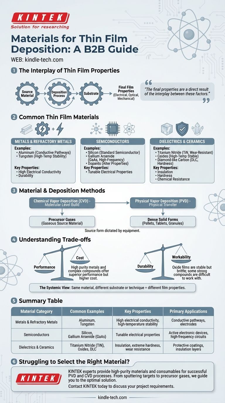
The materials used in thin film deposition are incredibly diverse, ranging from pure metals like aluminum to complex compound semiconductors like gallium arsenide (GaAs). The most common categories include metals, dielectrics, ceramics, and various forms of silicon. These materials are chosen for the specific electrical, optical, or mechanical properties they impart to a surface.

The choice of a thin film material is never made in isolation. The final properties of the film are a direct result of the interplay between the source material, the deposition process used to apply it, and the substrate it is applied to.

A Closer Look at Common Thin Film Materials

The material selected is the foundation of the thin film's function, whether it's for creating a semiconductor circuit, a wear-resistant coating, or an anti-reflective lens.

Metals and Refractory Metals

These materials are primarily used for their high electrical conductivity and durability.

Common examples include aluminum, which is a staple in microelectronics for creating conductive pathways. Refractory metals like tungsten are also used for their high-temperature stability.

Semiconductors

Semiconductors form the basis of virtually all modern electronics.

Silicon is the most widely used semiconductor material. Other critical materials include germanium, compound semiconductors like gallium arsenide (GaAs) for high-frequency applications, and various dopants introduced via ion implantation to alter electrical properties.

Dielectrics and Ceramics

These materials are valued for their insulating properties, hardness, and chemical resistance.

Nitrides, such as Titanium Nitride (TiN), provide extremely hard and wear-resistant coatings. Oxides are durable and can withstand high temperatures, while materials like diamond-like carbon (DLC) offer exceptional hardness and low friction.

The Critical Link: Materials and Deposition Methods

A material is only useful if it can be effectively applied. The physical form of the source material is often dictated by the deposition equipment it will be used in.

Chemical Vapor Deposition (CVD)

CVD builds films from the molecular level using chemical reactions.

This process relies on precursor gases that react and decompose on the substrate surface, meaning the source material must be in a gaseous state or easily vaporized.

Physical Vapor Deposition (PVD)

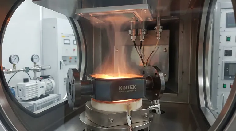
PVD involves physically transferring material from a source to a substrate, typically through evaporation or sputtering.

For these methods, the source material is often synthesized into a dense solid form, such as pellets, tablets, or granules, which can be heated or bombarded to release atoms.

Understanding the Trade-offs

Selecting a material always involves balancing competing factors. There is no single "best" material, only the most appropriate one for a specific goal and budget.

Performance vs. Cost

Highly pure metals and complex compounds offer superior performance but can be significantly more expensive and difficult to process.

The strength and durability of a metallic film, for example, must be weighed against its material and processing cost.

Durability vs. Workability

Some of the most durable materials present significant processing challenges.

Oxide films are exceptionally stable at high temperatures but can be brittle. Similarly, certain strong compound materials can be difficult to work with, requiring specialized equipment.

The Systemic View

It is critical to remember that the final film properties are not solely determined by the source material.

The same material deposited on a different substrate or using a different deposition technique can yield films with vastly different characteristics, including adhesion, stress, and density.

Making the Right Choice for Your Application

Your final material selection must be driven by the primary function of the thin film.

  • If your primary focus is electrical conductivity: Metals like aluminum or refractory metals like tungsten are the standard choices for interconnects and electrodes.
  • If your primary focus is hardness and wear resistance: Ceramics like Titanium Nitride (TiN) or coatings like diamond-like carbon (DLC) are ideal.
  • If your primary focus is creating active electronic devices: Silicon, compound semiconductors (GaAs), or specific dopants delivered via ion implantation are necessary.
  • If your primary focus is high-temperature stability or insulation: Oxides and other dielectric materials are the most suitable candidates.

Ultimately, successful thin film engineering depends on understanding that the material is just the starting point of a complex, interconnected system.

Summary Table:

Material Category Common Examples Key Properties Primary Applications
Metals & Refractory Metals Aluminum, Tungsten High electrical conductivity, high-temperature stability Conductive pathways, electrodes
Semiconductors Silicon, Gallium Arsenide (GaAs) Tunable electrical properties Active electronic devices, high-frequency circuits
Dielectrics & Ceramics Titanium Nitride (TiN), Oxides, DLC Insulation, extreme hardness, wear resistance Protective coatings, insulation layers

Struggling to select the right thin film material for your specific application? The experts at KINTEK are here to help. We specialize in providing the high-purity materials and consumables—from sputtering targets and evaporation pellets to precursor gases—that your lab needs for successful PVD and CVD processes. Let our deep application knowledge guide you to the optimal solution for conductivity, hardness, or thermal stability.

Contact KINTEK today to discuss your project requirements and discover how our materials can enhance your thin film performance.

Related Products

People Also Ask

Related Products

RF PECVD System Radio Frequency Plasma-Enhanced Chemical Vapor Deposition RF PECVD

RF PECVD System Radio Frequency Plasma-Enhanced Chemical Vapor Deposition RF PECVD

RF-PECVD is an acronym for "Radio Frequency Plasma-Enhanced Chemical Vapor Deposition." It deposits DLC (Diamond-like carbon film) on germanium and silicon substrates. It is utilized in the 3-12um infrared wavelength range.

Evaporation Boat for Organic Matter

Evaporation Boat for Organic Matter

The evaporation boat for organic matter is an important tool for precise and uniform heating during the deposition of organic materials.

Vacuum Hot Press Furnace Machine for Lamination and Heating

Vacuum Hot Press Furnace Machine for Lamination and Heating

Experience clean and precise lamination with Vacuum Lamination Press. Perfect for wafer bonding, thin-film transformations, and LCP lamination. Order now!

Custom Machined and Molded PTFE Teflon Parts Manufacturer for Laboratory ITO FTO Conductive Glass Cleaning Flower Basket

Custom Machined and Molded PTFE Teflon Parts Manufacturer for Laboratory ITO FTO Conductive Glass Cleaning Flower Basket

PTFE cleaning racks are mainly made of tetrafluoroethylene. PTFE, known as the "King of Plastics", is a polymer compound made of tetrafluoroethylene.

Rubber Vulcanizer Vulcanizing Machine Plate Vulcanizing Press for Lab

Rubber Vulcanizer Vulcanizing Machine Plate Vulcanizing Press for Lab

The Plate vulcanizing press is a kind of equipment used in the production of rubber products, mainly used for the vulcanization of rubber products. Vulcanization is a key step in rubber processing.

Hexagonal Boron Nitride HBN Ceramic Ring

Hexagonal Boron Nitride HBN Ceramic Ring

Boron nitride ceramic (BN) rings are commonly used in high temperature applications such as furnace fixtures, heat exchangers and semiconductor processing.

Single Punch Electric Tablet Press Machine Laboratory Powder Tablet Punching TDP Tablet Press

Single Punch Electric Tablet Press Machine Laboratory Powder Tablet Punching TDP Tablet Press

The single-punch electric tablet press is a laboratory-scale tablet press suitable for corporate laboratories in pharmaceutical, chemical, food, metallurgical and other industries.

Precision Machined Silicon Nitride (SiN) Ceramic Sheet for Engineering Advanced Fine Ceramics

Precision Machined Silicon Nitride (SiN) Ceramic Sheet for Engineering Advanced Fine Ceramics

Silicon nitride plate is a commonly used ceramic material in the metallurgical industry due to its uniform performance at high temperatures.

Silicon Carbide (SIC) Ceramic Sheet Wear-Resistant Engineering Advanced Fine Ceramics

Silicon Carbide (SIC) Ceramic Sheet Wear-Resistant Engineering Advanced Fine Ceramics

Silicon carbide (sic) ceramic sheet is composed of high-purity silicon carbide and ultra-fine powder, which is formed by vibration molding and high-temperature sintering.

Professional Cutting Tools for Carbon Paper Cloth Diaphragm Copper Aluminum Foil and More

Professional Cutting Tools for Carbon Paper Cloth Diaphragm Copper Aluminum Foil and More

Professional tools for cutting lithium sheets, carbon paper, carbon cloth, separators, copper foil, aluminum foil, etc., with round and square shapes and different sizes of blades.

Small Lab Rubber Calendering Machine

Small Lab Rubber Calendering Machine

Small lab rubber calendering machine is used for producing thin, continuous sheets of plastic or rubber materials. It is commonly employed in laboratories, small-scale production facilities, and prototyping environments to create films, coatings, and laminates with precise thickness and surface finish.

Custom PTFE Teflon Parts Manufacturer for Conductive Glass Substrate Cleaning Rack

Custom PTFE Teflon Parts Manufacturer for Conductive Glass Substrate Cleaning Rack

The PTFE conductive glass substrate cleaning rack is used as the carrier of the square solar cell silicon wafer to ensure efficient and pollution-free handling during the cleaning process.

Advanced Engineering Fine Ceramics Boron Nitride (BN) Ceramic Parts

Advanced Engineering Fine Ceramics Boron Nitride (BN) Ceramic Parts

Boron nitride ((BN) is a compound with high melting point, high hardness, high thermal conductivity and high electrical resistivity. Its crystal structure is similar to graphene and harder than diamond.

Custom PTFE Teflon Parts Manufacturer for PTFE Mesh F4 Sieve

Custom PTFE Teflon Parts Manufacturer for PTFE Mesh F4 Sieve

PTFE mesh sieve is a specialized test sieve designed for particle analysis in various industries, featuring a non-metallic mesh woven from PTFE filament. This synthetic mesh is ideal for applications where metal contamination is a concern . PTFE sieves are crucial for maintaining the integrity of samples in sensitive environments, ensuring accurate and reliable results in particle size distribution analysis.

Aluminum Foil Current Collector for Lithium Battery

Aluminum Foil Current Collector for Lithium Battery

The surface of aluminum foil is extremely clean and hygienic, and no bacteria or microorganisms can grow on it. It is a non-toxic, tasteless and plastic packaging material.

High-Purity Titanium Foil and Sheet for Industrial Applications

High-Purity Titanium Foil and Sheet for Industrial Applications

Titanium is chemically stable, with a density of 4.51g/cm3, which is higher than aluminum and lower than steel, copper, and nickel, but its specific strength ranks first among metals.

Custom PTFE Teflon Parts Manufacturer for Centrifuge Tube Racks

Custom PTFE Teflon Parts Manufacturer for Centrifuge Tube Racks

The precision-made PTFE test tube racks are completely inert and, due to the high temperature properties of PTFE, these test tube racks can be sterilized (autoclaved) without any problems.


Leave Your Message