Of the common PVD methods, Pulsed Laser Deposition (PLD) is renowned for its ability to produce films with exceptional stoichiometric purity. This is because the high-energy laser pulse ablates a target, transferring the material to the substrate in a way that often preserves the exact chemical composition of complex, multi-element materials like the Boron Carbide (B4C) mentioned in your reference.
The choice of a PVD technique for high purity is not about finding a single "best" method, but about understanding the fundamental deposition mechanism of each process. PLD excels at preserving complex stoichiometry, while other methods like sputtering offer different advantages in scalability and control for simpler materials.
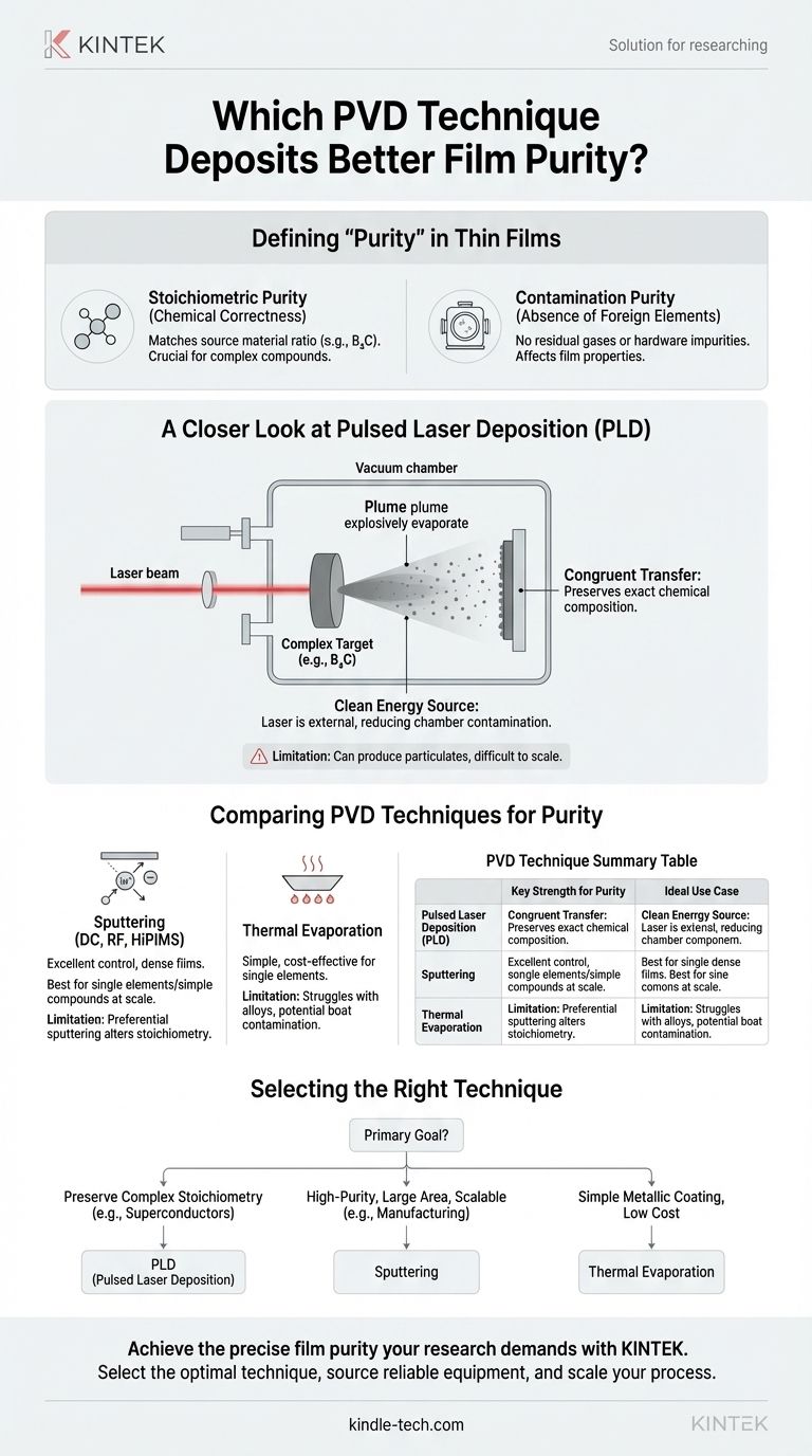
What Defines "Purity" in Thin Films?
Before comparing techniques, we must define purity in two distinct ways. Both are critical for film performance.
Stoichiometric Purity
This refers to the chemical correctness of the film. It means the ratio of different elements in the deposited film (e.g., the ratio of Boron to Carbon in B₄C) perfectly matches the ratio in the source material.
Maintaining stoichiometry is a major challenge when depositing compounds or alloys, as different elements can have vastly different physical properties.
Contamination Purity
This is the absence of unwanted foreign elements in the film. Contaminants can come from several sources, including residual gases in the vacuum chamber, the chamber walls, or even the deposition hardware itself.
Even trace amounts of contaminants can drastically alter a film's electronic, optical, or mechanical properties.
A Closer Look at Pulsed Laser Deposition (PLD)
PLD's reputation for high purity stems directly from its unique physical process.
The Principle of Congruent Transfer
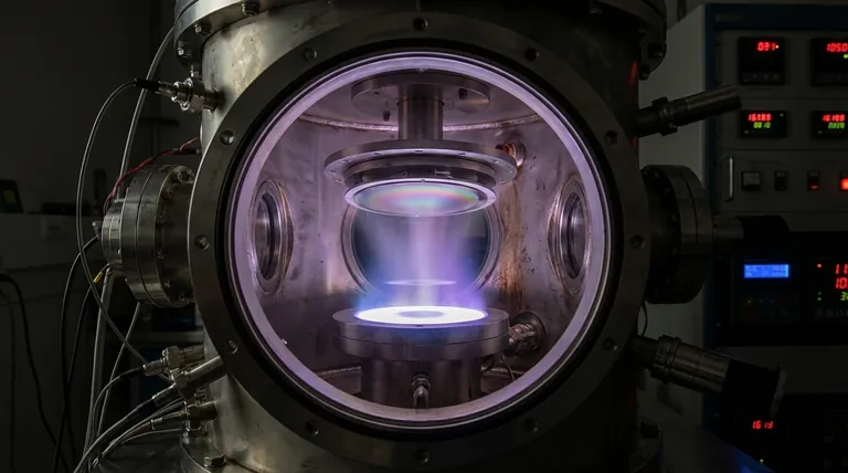
PLD uses a high-power laser focused on a target material inside a vacuum chamber. The intense, short laser pulse causes a rapid, explosive evaporation (or "ablation") of the target surface.
This process is so fast that it tends to transfer all elements from the target to the substrate at the same time, regardless of their individual melting points or vapor pressures. This is called congruent transfer and is the primary reason PLD excels at maintaining the stoichiometry of complex materials.
A Clean Energy Source
The energy source in PLD—the laser—is located outside the vacuum chamber. This means there are fewer hot filaments or high-voltage electrodes inside the chamber that could outgas or become a source of contamination compared to other PVD techniques.
Comparing Purity Across PVD Techniques
While PLD is excellent for stoichiometry, other common PVD methods have their own strengths and are often used to achieve high purity for different types of materials.
Sputtering (DC, RF, HiPIMS)
In sputtering, ions from a plasma (usually Argon) bombard a target, knocking atoms off the surface which then deposit onto the substrate.
Sputtering offers excellent control and can produce very dense, high-purity films, especially for single elements or simple compounds. However, for complex targets, it can suffer from "preferential sputtering," where one element is removed more easily than another, altering the film's stoichiometry.
Thermal Evaporation
This is one of the simplest PVD methods. A source material is heated in a crucible (a "boat") until it evaporates and condenses on the substrate.
This method struggles with alloys or compounds. The element with the higher vapor pressure will evaporate first, leading to a film with a chemical composition that changes throughout its thickness and differs significantly from the source. Contamination from the heated boat can also be a concern.
Understanding the Trade-offs
No single technique is perfect for every application. The choice always involves balancing competing factors.
PLD's Limitations
While excellent for purity, PLD is notorious for producing microscopic droplets or "particulates" that can land on the film, creating defects. It is also very difficult to scale up for coating large areas (e.g., large silicon wafers or architectural glass), limiting its use primarily to research and development.
Sputtering's Strengths
Sputtering is the workhorse of the semiconductor and manufacturing industries for a reason. It provides excellent uniformity over large areas, is highly reliable, and is a very mature, well-understood process. For metals and many simple compounds, it is the clear choice for industrial-scale production of high-purity films.
Evaporation's Niche
Thermal evaporation is often the simplest and cheapest method. It is highly effective for depositing single-element films where perfect density or minimal contamination is not the absolute top priority, such as creating simple metallic contacts.
Selecting the Right Technique for High Purity
Your final decision must be guided by the specific material you are depositing and your primary goal.
- If your primary focus is preserving the exact stoichiometry of a complex, multi-element material (like a superconductor or specific carbide): PLD is often the superior choice due to its congruent material transfer.
- If your primary focus is depositing a high-purity single element or simple compound over a large, uniform area for manufacturing: A well-controlled Sputtering system is a highly reliable and scalable option.
- If your primary focus is a simple metallic coating where cost and simplicity are the main drivers: Thermal Evaporation is a viable starting point, but you must accept potential compromises in stoichiometric purity.
Ultimately, achieving high purity is a function of choosing the right physical process for your specific material and application.
Summary Table:
| PVD Technique | Key Strength for Purity | Ideal Use Case |
|---|---|---|
| Pulsed Laser Deposition (PLD) | Congruent transfer preserves complex stoichiometry | Multi-element compounds (e.g., B₄C, superconductors) |
| Sputtering | High purity for single elements, excellent uniformity | Industrial-scale metal/simple compound films |
| Thermal Evaporation | Simplicity, cost-effectiveness | Basic metallic coatings where purity is less critical |
Achieve the precise film purity your research demands with KINTEK.
Whether you're developing advanced materials requiring perfect stoichiometry or scaling up a manufacturing process, selecting the right PVD equipment is critical. KINTEK specializes in high-performance lab equipment, including PVD systems tailored for both research and production environments.
We can help you:
- Select the optimal PVD technique (PLD, Sputtering, or Evaporation) for your specific material and purity requirements
- Source reliable equipment that delivers consistent, contaminant-free results
- Scale your process from R&D to manufacturing with uniform, high-purity coatings
Ready to enhance your thin-film capabilities? Contact our experts today for a personalized consultation on the best PVD solution for your laboratory needs.
Visual Guide
Related Products
- RF PECVD System Radio Frequency Plasma-Enhanced Chemical Vapor Deposition RF PECVD
- HFCVD Machine System Equipment for Drawing Die Nano-Diamond Coating
- Chemical Vapor Deposition CVD Equipment System Chamber Slide PECVD Tube Furnace with Liquid Gasifier PECVD Machine
- 915MHz MPCVD Diamond Machine Microwave Plasma Chemical Vapor Deposition System Reactor
- VHP Sterilization Equipment Hydrogen Peroxide H2O2 Space Sterilizer
People Also Ask
- What is an example of PECVD? RF-PECVD for High-Quality Thin Film Deposition
- How are PECVD and CVD different? A Guide to Choosing the Right Thin-Film Deposition Process
- Why is PECVD environment friendly? Understanding the Eco-Friendly Benefits of Plasma-Enhanced Coating
- What are the applications of PECVD? Essential for Semiconductors, MEMS, and Solar Cells
- What are the benefits of PECVD? Achieve Superior Low-Temperature Thin Film Deposition