At its core, electron beam (e-beam) evaporation was developed to overcome the fundamental limitations of simpler thermal evaporation methods. It provides a way to deposit higher-purity, higher-density thin films from a much wider range of materials, including those with very high melting points. This level of control is critical for producing advanced optical, semiconductor, and architectural products.
E-beam evaporation solves a critical problem: how to vaporize a material without contaminating it or being limited by the melting point of a heating element. By using a focused beam of electrons as the heat source, it enables the deposition of materials and film qualities that are impossible to achieve with conventional resistive heating.
The Limits of Simpler Evaporation
To understand the value of e-beam evaporation, you must first understand the method it improved upon: resistive thermal evaporation.
The Conventional Method: Resistive Heating
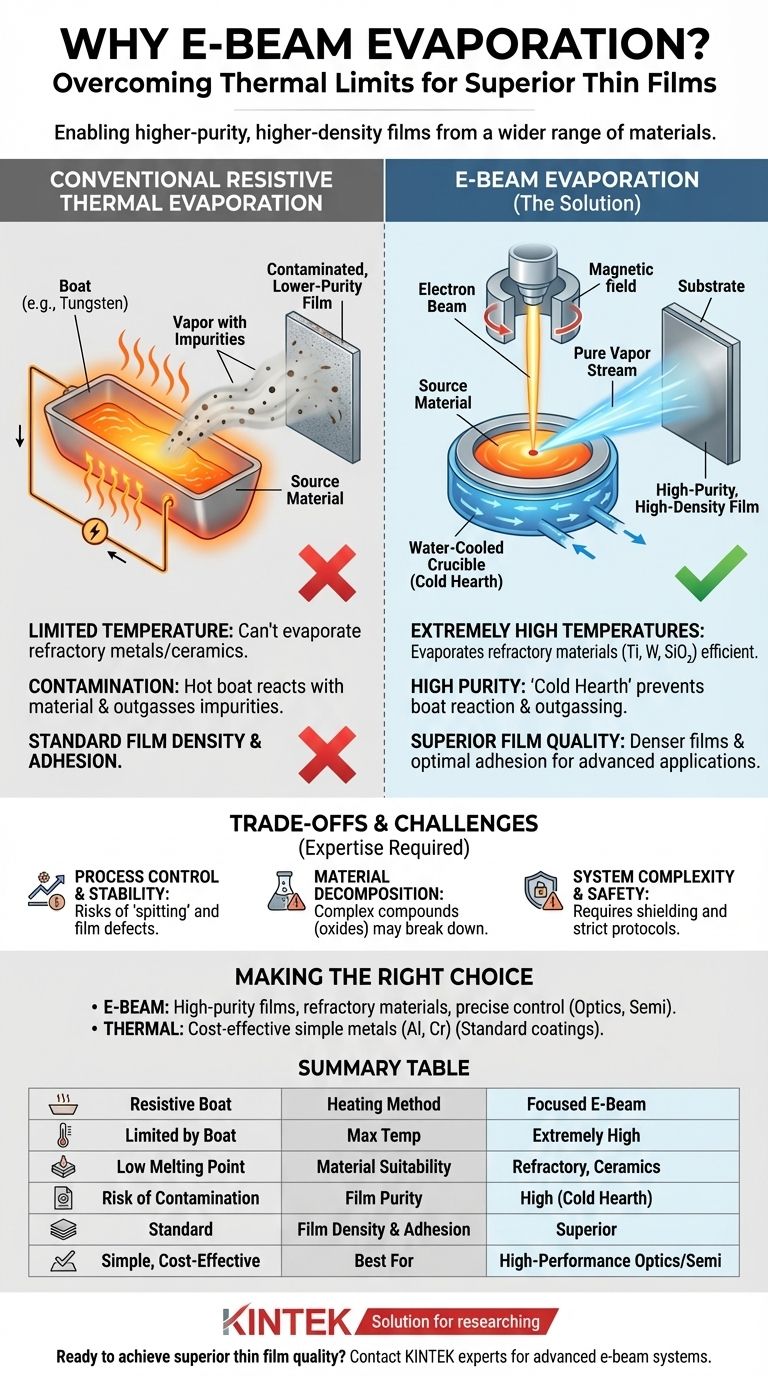
In traditional thermal evaporation, a small container, often called a "boat" and typically made of a refractory metal like tungsten, is filled with the source material. An electric current is passed through this boat, causing it to heat up like the filament in a light bulb.
This heat is transferred to the source material, causing it to melt and then evaporate. While simple, this approach has significant drawbacks.
The Problem of Temperature and Contamination
The primary limitation is that the boat must get hotter than the material it's evaporating. This creates two problems.
First, you are limited to evaporating materials with melting points lower than that of the boat itself. This makes it impossible to deposit refractory metals or many ceramic compounds.
Second, the extremely hot boat can react with the source material or release its own impurities (outgassing). These impurities mix with the material vapor, resulting in a contaminated, lower-purity thin film on your substrate.
How E-Beam Evaporation Solves These Problems
E-beam evaporation fundamentally redesigns the heating process to eliminate the issues of temperature limits and contamination.
A Focused, High-Energy Source
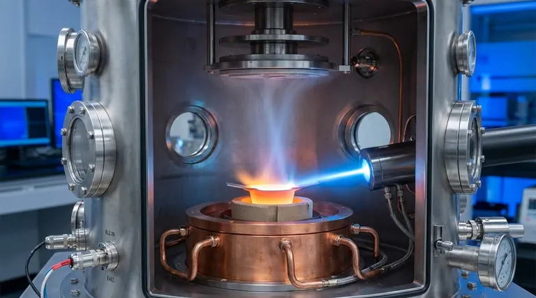
Instead of heating a container, this method uses a high-energy electron beam, guided by magnetic fields, to directly strike the surface of the source material.
This beam acts as a surgical heat source, focusing immense energy onto a very small spot.
Unlocking High-Melting-Point Materials
Because the energy is delivered directly to the source material, it can reach temperatures far greater than what a resistive boat could withstand.
This allows for the efficient evaporation of materials with extremely high melting points, such as titanium, tungsten, and oxides like silica, which are essential for optical coatings and durable electronics.
The "Cold Hearth" Advantage
Crucially, the crucible (or "hearth") holding the bulk of the source material is actively water-cooled. Only the top surface layer targeted by the electron beam becomes molten.
This "cold hearth" approach means the container never gets hot enough to react with the source material or outgas. The result is a significantly purer vapor stream and a higher-quality deposited film.
Superior Film Quality
The intense, localized heating of e-beam evaporation produces a more energetic vapor. These energetic atoms or molecules arrive at the substrate with more kinetic energy.
This leads to denser thin films and optimal substrate adhesion, which are critical properties for performance and durability in applications like laser optics and semiconductor devices.
Understanding the Trade-offs and Challenges
While powerful, e-beam evaporation is a more complex process with its own set of challenges. An expert must be aware of these trade-offs.
Process Control and Stability
The intense, localized heating can sometimes be unstable. It can cause solid material to fracture and be ejected, an issue known as "spitting," which can create defects in the film.
Balancing the power of the beam and the amount of material in the crucible requires significant process expertise.
Material Decomposition
The high energy of the electron beam is not always benign. For certain complex compounds, particularly oxides, the intense heat can cause the material to decompose or reduce.
This means the resulting vapor may not have the same chemical composition as the starting material, requiring careful process tuning to manage.
System Complexity and Safety
E-beam systems are more complex and expensive than simple thermal evaporators. Furthermore, the impact of high-energy electrons on a target material generates X-rays, which necessitates proper lead shielding and rigorous safety protocols for operators.
Making the Right Choice for Your Application
Your choice of evaporation technique should be driven by the specific requirements of your final product.
- If your primary focus is high-purity films or refractory materials: E-beam evaporation is the definitive choice for its purity and ability to handle high-melting-point sources.
- If your primary focus is cost-effective deposition of simple metals (e.g., aluminum, chrome): Standard resistive thermal evaporation is often sufficient and more economical.
- If your primary focus is precise control over optical properties or film density: E-beam evaporation provides the superior control over deposition rate and film structure required for advanced coatings.
Ultimately, e-beam evaporation provides a level of material versatility and film quality control that is indispensable for manufacturing modern, high-performance devices.
Summary Table:
| Feature | Conventional Thermal Evaporation | E-Beam Evaporation |
|---|---|---|
| Heating Method | Resistive heating of a boat/crucible | Focused electron beam directly on material |
| Max Temperature | Limited by boat material melting point | Extremely high, not limited by a container |
| Material Suitability | Lower melting point metals (e.g., Al, Cr) | Refractory metals, ceramics, oxides (e.g., W, SiO₂) |
| Film Purity | Risk of contamination from the hot boat | High purity due to water-cooled "cold hearth" |
| Film Density & Adhesion | Standard | Superior, due to more energetic vapor |
| Best For | Cost-effective, simple metal deposition | High-performance optical, semiconductor, and architectural coatings |
Ready to achieve superior thin film quality for your lab's most demanding projects?
At KINTEK, we specialize in providing advanced lab equipment, including e-beam evaporation systems, to help you deposit high-purity, high-density films from even the most challenging materials. Whether you're developing advanced semiconductors, precision optical coatings, or durable architectural layers, our expertise ensures you get the performance and reliability your research requires.
Let's discuss how our solutions can enhance your thin film processing. Contact our experts today for a personalized consultation!
Visual Guide
Related Products
- Electron Beam Evaporation Coating Tungsten Crucible and Molybdenum Crucible for High Temperature Applications
- Electron Beam Evaporation Coating Oxygen-Free Copper Crucible and Evaporation Boat
- Electron Beam Evaporation Coating Gold Plating Tungsten Molybdenum Crucible for Evaporation
- Electron Beam Evaporation Coating Conductive Boron Nitride Crucible BN Crucible
- E Beam Crucibles Electron Gun Beam Crucible for Evaporation
People Also Ask
- What are the applications of e-beam evaporation? Achieve High-Purity Coatings for Optics & Electronics
- What is the container that holds the metal source material called in e-beam evaporation? Ensure Purity and Quality in Your Thin-Film Deposition
- What is e-beam evaporation? Achieve High-Purity Thin Film Deposition for Your Lab
- What is e-beam evaporation used for? Precision Coating for Optics, Aerospace & Electronics
- What is the voltage of e-beam evaporation? Achieve Precise Thin-Film Deposition


