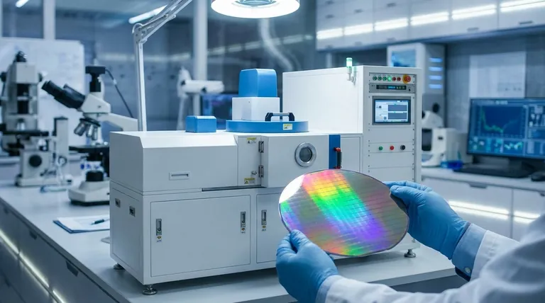
In materials science and advanced manufacturing, film thickness is not merely a dimensional measurement; it is the most critical parameter dictating a material's core function. The thickness of a thin film—a layer of material ranging from a few nanometers to several micrometers—directly governs its physical, optical, and electrical properties. For this reason, controlling thickness is essential for ensuring products like semiconductor devices, optical lenses, and solar panels function with precision, meet design specifications, and maintain reliability.
Beyond being a simple quality check, film thickness is the primary control lever for a material's functional behavior. An incorrect thickness doesn't just create a minor defect; it fundamentally alters how the component interacts with light, electricity, and its physical environment, often leading to complete device failure.
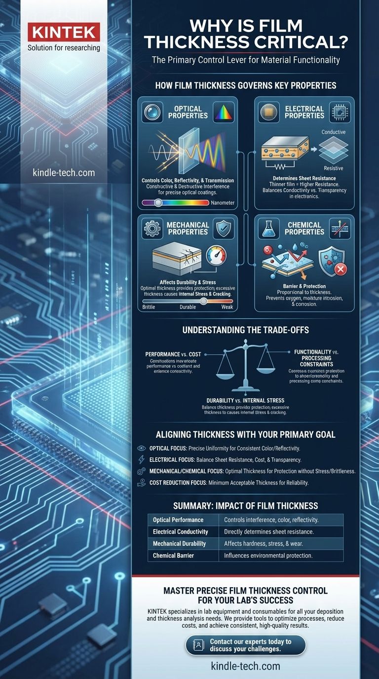
How Film Thickness Governs Key Properties
The importance of film thickness becomes clear when you understand its direct impact on a material's most fundamental characteristics. A change of even a few nanometers can be the difference between a functional product and a failed one.
Optical Properties: Color, Reflectivity, and Transmission
For optical coatings, thickness is everything. When light waves strike a thin film, they reflect off both the top and bottom surfaces. These reflected waves interfere with each other.
Depending on the film's thickness, this interference can be constructive (amplifying certain colors) or destructive (canceling out others). This phenomenon, known as thin-film interference, is precisely how anti-reflection coatings on eyeglasses work.
By controlling thickness, engineers can dial in the exact color, transmission, and reflectivity required for applications like camera lenses, architectural glass, and optical filters.
Electrical Properties: Conductivity and Resistance
In electronics and semiconductors, the thickness of a conductive or semi-conductive layer directly correlates to its sheet resistance. A thinner film has fewer charge carriers in its cross-section, resulting in higher electrical resistance.
This principle is critical in manufacturing transparent conductive films for touch screens and OLED displays, where a balance must be struck between conductivity (requiring more thickness) and transparency (requiring less). In photovoltaics, the thickness of each layer in the solar cell is optimized to ensure efficient absorption of light and extraction of electrical current.
Mechanical Properties: Durability and Stress
Thin films are often applied as protective coatings to improve a product's durability, wear resistance, or hardness. While a thicker coating may seem more robust, it can also introduce significant internal stress.
This stress builds up during the deposition process and can cause the film to crack, peel, or delaminate from the substrate, compromising its protective function. The optimal thickness provides the necessary durability without succumbing to stress-related failure.
Chemical Properties: Barrier and Protection
Many films serve as a barrier to protect a substrate from its environment. This is common in food packaging to prevent oxygen and moisture intrusion and in medical devices to create a biocompatible, inert surface.
The effectiveness of this barrier is directly proportional to the film's thickness and density. A film that is too thin may contain pinholes or be too permeable, failing to provide adequate protection.
Understanding the Trade-offs of Film Thickness
Optimizing film thickness is rarely about maximizing it. Instead, it is a delicate balancing act between competing requirements. Understanding these trade-offs is key to efficient and successful product design.
Performance vs. Cost
Thicker films require more raw material and typically increase the deposition time, both of which drive up manufacturing costs. The goal is always to identify the minimum acceptable thickness that meets all critical performance specifications without over-engineering the component.
Durability vs. Internal Stress
As noted, increasing thickness to improve hardness or wear resistance can backfire. The buildup of internal stress in a thicker film can make it brittle and more prone to cracking than a slightly thinner, more compliant layer.
Functionality vs. Processing Constraints
In some manufacturing processes, such as semiconductor lithography, the thickness of one layer directly affects the ability to process the next. A photoresist layer that is too thick may be difficult to pattern accurately, while one that is too thin may not provide enough protection during an etching step.
Aligning Thickness with Your Primary Goal
The "right" thickness is entirely dependent on your application's end goal. To make a sound decision, you must first define your primary objective.
- If your primary focus is optical performance: Your goal is precise control over light interference, so you must maintain thickness uniformity to achieve consistent color and reflectivity.
- If your primary focus is electrical conductivity: You must balance the required sheet resistance with material cost and optical transparency, as thickness directly controls this relationship.
- If your primary focus is mechanical protection or a chemical barrier: You must find the optimal thickness that provides sufficient protection without introducing excessive internal stress or brittleness.
- If your primary focus is cost reduction: The objective is to identify the absolute minimum thickness that still meets all critical performance specifications for the product to function reliably.
Ultimately, mastering film thickness is mastering control over your final product's performance, cost, and reliability.
Summary Table:
| Key Property | Impact of Film Thickness |
|---|---|
| Optical Performance | Controls color, reflectivity, and transmission via thin-film interference. |
| Electrical Conductivity | Directly determines sheet resistance in semiconductors and displays. |
| Mechanical Durability | Affects hardness, wear resistance, and internal stress. |
| Chemical Barrier | Influences protection against moisture, oxygen, and corrosion. |
Master precise film thickness control for your lab's success.
Film thickness is not just a measurement—it's the foundation of your product's functionality, from semiconductor devices to protective coatings. Ensuring precise, reliable control is critical for performance and yield.
KINTEK specializes in lab equipment and consumables for all your deposition and thickness analysis needs. We provide the tools and expertise to help you optimize your processes, reduce costs, and achieve consistent, high-quality results.
Ready to achieve unparalleled control over your material properties? Contact our experts today to discuss how our solutions can meet the specific challenges of your laboratory.
Visual Guide
Related Products
- Small Lab Rubber Calendering Machine
- Lab Plastic PVC Calender Stretch Film Casting Machine for Film Testing
- Lab Blown Film Extrusion Three Layer Co-Extrusion Film Blowing Machine
- XRD Sample Holder X-ray Diffractometer Powder Slide
- Filter Testing Machine FPV for Dispersion Properties of Polymers and Pigments
People Also Ask
- What is the principle of calendering? Enhance Fabric Surface with Heat and Pressure
- What is the sputtering yield of materials? Master Deposition Rates & Film Quality
- What is the principle of wiped film molecular still? Preserve and Purify Heat-Sensitive Compounds
- What is the process of calendering? A Guide to High-Volume Plastic Film Production
- What are the factors affecting sputtering yield? Master Your Deposition Rate & Film Quality