In short, sputtering is slower because its mechanism is fundamentally less efficient at liberating material. Sputtering uses energetic ions to physically knock atoms off a target one by one, a process governed by momentum transfer. Thermal evaporation, in contrast, heats a source material until it creates a dense, high-volume vapor stream through a bulk phase change, releasing a far greater number of atoms in the same amount of time.
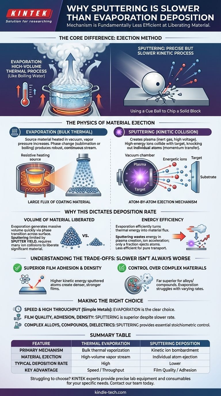
The core difference lies in the method of material ejection. Evaporation is a high-volume thermal process, like boiling water to create steam. Sputtering is a precise but slower kinetic process, like using a cue ball to chip away at a solid block.
The Physics of Material Ejection
To understand the difference in deposition rates, we must look at how each physical vapor deposition (PVD) method transforms a solid source material into a vapor. The two approaches could not be more different.
Evaporation: A Bulk Thermal Process
In thermal evaporation, the source material is heated in a high vacuum, typically using resistive heating or an electron beam.
As the material's temperature rises, its vapor pressure increases. Once it reaches a sufficient temperature, it undergoes a phase change (sublimation or boiling), producing a robust and continuous stream of vapor that travels to and condenses on the substrate. This is a highly effective way to generate a large flux of coating material.
Sputtering: A Kinetic Collision Process
Sputtering does not rely on heat to create a vapor. Instead, it creates a plasma by introducing an inert gas (like Argon) into the vacuum chamber and applying a high voltage.
Positively charged ions from the plasma are accelerated towards the negatively charged source material, known as the target. When these high-energy ions collide with the target, they transfer their momentum, physically knocking out, or "sputtering," individual atoms or small clusters. This is an atom-by-atom ejection mechanism.
Why This Mechanism Difference Dictates Deposition Rate
The fundamental physics of each process directly impacts the resulting speed.
Volume of Material Liberated
Evaporation's strength is its ability to generate a massive volume of vapor quickly. The energy input is used to cause a phase transition across the surface of the source material, releasing an enormous number of atoms simultaneously.
Sputtering is limited by the sputter yield—the number of target atoms ejected per incident ion. This yield is often a low number, meaning many ion collisions are required to liberate a significant amount of material, making the process inherently slower.
Energy Efficiency
In evaporation, the thermal energy is applied directly to generate vapor. The process is relatively efficient at turning energy into a material flux.
In sputtering, the electrical energy is used to create and sustain a plasma, accelerate ions, and bombard the target. Only a fraction of an ion's kinetic energy results in the successful ejection of a target atom. This multi-step, momentum-transfer process is simply less efficient for pure material transport.
Understanding the Trade-offs: Why Slower Isn't Always Worse
A higher deposition rate does not automatically make evaporation the superior technique. The slower, more controlled nature of sputtering provides critical advantages in film quality.
Superior Film Adhesion and Density
Sputtered atoms are ejected with significantly higher kinetic energy (1-10 eV) compared to evaporated atoms (~0.1 eV). When these energetic atoms arrive at the substrate, they create denser, more uniform, and more strongly adhered films.
Control Over Complex Materials
Sputtering is far superior for depositing alloys or compound materials. Because it chips atoms off the target, the resulting vapor has a composition that is very close to the target material itself. Evaporation can struggle with this, as different elements in an alloy will evaporate at different rates.
Making the Right Choice for Your Application
Choosing between these methods requires you to weigh the need for speed against the demand for film quality.
- If your primary focus is speed and high throughput for simple metal coatings: Evaporation is the clear choice due to its high-volume vapor generation.
- If your primary focus is film quality, adhesion, and density: Sputtering's controlled, energetic deposition is superior, despite the slower rate.
- If you are depositing complex alloys, compounds, or dielectrics: Sputtering provides the essential stoichiometric control that evaporation often lacks.
Ultimately, understanding the physics behind each method allows you to select the right tool not for its speed, but for its ability to produce the specific film properties your application demands.
Summary Table:
| Feature | Thermal Evaporation | Sputtering Deposition |
|---|---|---|
| Primary Mechanism | Bulk thermal vaporization | Kinetic ion bombardment |
| Material Ejection | High-volume vapor stream | Individual atom ejection |
| Typical Deposition Rate | High | Lower |
| Key Advantage | Speed / Throughput | Film Quality / Adhesion |
Struggling to choose the right deposition technology for your thin-film application? The experts at KINTEK understand that the decision between speed and quality is critical. Whether your project demands the high throughput of evaporation or the superior film properties of sputtering, we provide the precise lab equipment and consumables you need.
Contact our team today to discuss your specific requirements and let KINTEK's solutions enhance your laboratory's capabilities and research outcomes.
Visual Guide