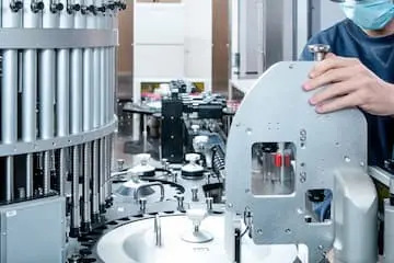
PECVD (Plasma Enhanced Chemical Vapor Deposition) Machine is a tool used in the semiconductor industry for depositing thin films on a substrate. The machine uses low-temperature plasma to generate a glow discharge to warm up the sample and introduce an appropriate amount of process gas. The process involves chemical and plasma reactions to form a solid film on the surface of the sample. PECVD equipment is mainly composed of vacuum and pressure control systems, precipitation systems, gas and flow control, computer control, and safety protection systems. The machine is used for continuous coating and modification of powder materials by CVD method in an atmosphere-protected environment.
Toggle Categories
Get Instant Support
Choose your preferred way to connect with our team
-
Get Free Quote Fill out form for detailed pricing
-
Send Email Detailed inquiry support
-
WhatsApp Quick mobile chat
Response Time
Within 8 hours on working days, 24 hours on holidays
pecvd machine

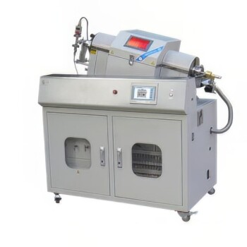


RF PECVD System Radio Frequency Plasma-Enhanced Chemical Vapor Deposition RF PECVD
Item Number : KT-RFPE
Our extensive portfolio guarantees that we have an appropriate standard solution that will meet your needs. We also offer bespoke design services to meet unique customer requirements. Our PECVD machines are essential tools in modern semiconductor manufacturing, offering excellent film uniformity, low-temperature processing, and high throughput. Our machines are used in a wide range of applications, including the deposition of thin films for microelectronic devices, photovoltaic cells, and display panels.
Applications of PECVD Machine
- Deposition of thin films for microelectronic devices
- Photovoltaic cell production
- Display panel manufacturing
- Silicon dioxide film deposition
- Silicon nitride film deposition
- Amorphous silicon film deposition
- Deposition of films on substrates with low thermal budgets
- Production of power semiconductor devices
- Production of optoelectronics
- Use in data centers
- 5G network equipment production
- Autonomous vehicle equipment manufacturing
- Renewable energy device production
- Electronic warfare equipment production
- Smart lighting manufacturing
Advantages of PECVD Machine
- Low deposition temperatures
- Good conformity and step coverage on uneven surfaces
- Tighter control of the thin film process
- High deposition rates
- Suitable for the fabrication of films with different compositions and microstructures, allowing one to continuously vary film characteristics as a function of depth
- Provides high deposition rates, substantially higher than other, more traditional vacuum-based techniques
- Different substrate shapes (including 3D) can be uniformly coated
- The films being deposited have low mechanical stress
- Good conformal step coverage and excellent uniformity of the films thickness over the step edge and flat surface
- Deposits thin films with good dielectric properties
- High-efficiency electrical performance and bonding to very high standards
Our PECVD machine is a cost-effective solution for all your thin-film deposition needs. With our extensive product line, we provide you with a standard solution that fits your needs, and for more unique applications, our custom design service will help us cater to your specific requirements.
FAQ
What Is PECVD Method?
PECVD (Plasma Enhanced Chemical Vapor Deposition) is a process used in semiconductor manufacturing to deposit thin films on microelectronic devices, photovoltaic cells, and display panels. In PECVD, a precursor is introduced to the reaction chamber in a gaseous state, and the assistance of plasma reactive media dissociates the precursor at much lower temperatures than with CVD. PECVD systems offer excellent film uniformity, low-temperature processing, and high throughput. They are used in a wide range of applications and will play an increasingly important role in the semiconductor industry as the demand for advanced electronic devices continues to grow.
What Is PECVD Used For?
PECVD (Plasma Enhanced Chemical Vapor Deposition) is widely used in the semiconductor industry to fabricate integrated circuits, as well as in the photovoltaic, tribological, optical, and biomedical fields. It is used to deposit thin films for microelectronic devices, photovoltaic cells, and display panels. PECVD can produce unique compounds and films that cannot be created by common CVD techniques alone, and films that demonstrate high solvent and corrosion resistance with chemical and thermal stability. It is also used to produce homogenous organic and inorganic polymers over large surfaces, and Diamond-like Carbon (DLC) for tribological applications.
What Are The Advantages Of PECVD?
The primary advantages of PECVD are its ability to operate at lower deposition temperatures, providing better conformity and step coverage on uneven surfaces, tighter control of the thin film process, and high deposition rates. PECVD allows for successful applications in situations where conventional CVD temperatures could potentially damage the device or substrate being coated. By operating at a lower temperature, PECVD creates less stress between thin film layers, allowing for high-efficiency electrical performance and bonding to very high standards.
What Is The Difference Between ALD And PECVD?
ALD is a thin film deposition process that allows for atomic layer thickness resolution, excellent uniformity of high aspect ratio surfaces and pinhole-free layers. This is achieved by the continuous formation of atomic layers in a self-limiting reaction. PECVD, on the other hand, involves mixing the source material with one or more volatile precursors using a plasma to chemically interact and breakdown the source material. The processes use heat with higher pressures leading to a more reproducible film where the film thicknesses could be managed by time/power. These films are more stoichiometric, denser and are capable of growing higher quality insulator films.
What Is The Difference Between PECVD And Sputtering?
PECVD and sputtering are both physical vapor deposition techniques used for thin film deposition. PECVD is a diffusive gas-driven process that yields very high-quality thin films while sputtering is a line-of-sight deposition. PECVD allows for better coverage on uneven surfaces such as trenches, walls, and high conformity and can produce unique compounds and films. On the other hand, sputtering is good for the deposition of fine layers of several materials, ideal for creating multi-layered and multi-graduated coating systems. PECVD is mainly used in the semiconductor industry, tribological, optical, and biomedical fields while sputtering is mostly used for dielectric materials and tribological applications.
REQUEST A QUOTE
Our professional team will reply to you within one business day. Please feel free to contact us!
Related Articles

How to Select the Right Oil-Free Diaphragm Pump for Your Lab or Industrial Needs
Learn how to choose the right oil-free diaphragm pump for your lab or industry—balancing specs, chemical resistance, and lifetime costs.
Read more
How Cascade Refrigeration Powers Ultra-Low Temperature Freezers Beyond Single-Stage Limits
Learn how cascade refrigeration enables ultra-low temperature freezers to reach -80°C and beyond, overcoming single-stage system limitations for critical sample storage.
Read more
Upright vs. Chest ULT Freezers: How to Choose the Right Configuration for Your Lab
Compare upright vs. chest ULT freezers for your lab: temperature stability, workflow efficiency, and cost analysis to protect sensitive samples.
Read more
How ULT Freezers Prevent Catastrophic Loss of Microbiological Samples
ULT freezers safeguard microbiological samples with advanced temperature control, contamination prevention, and emergency backup systems to prevent catastrophic loss.
Read more
How ULT Freezers Protect Scientific Discoveries in Genetics and Drug Development
ULT freezers safeguard genetic and pharmaceutical research by maintaining -80°C storage for DNA, proteins, and cell lines—preventing sample degradation and ensuring research validity.
Read more
Preserving the Irreplaceable: How ULT Freezers Protect Critical Samples Across Industries
ULT freezers at -80°C protect biological samples, vaccines, and research materials from degradation, ensuring long-term viability across industries.
Read more
PTFE gasket: an all-around solution for flange sealing
Polytetrafluoroethylene (PTFE) gaskets have become an ideal choice in the field of flange sealing due to their unique chemical stability and high temperature resistance.
Read more
Factors in Selecting Large Optical Windows
Considerations for choosing large optical windows, including material, polishing, and coating.
Read more
Electron Beam Evaporation Coating Technology and Material Selection
An in-depth look at the principles and applications of electron beam evaporation coating technology, including material selection and various fields of application.
Read more
Electron Beam Evaporation: Advanced Thin Film Creation
Explores the technology and applications of electron beam evaporation in thin film production.
Read more
Electron Beam Evaporation Coating: Principles, Characteristics, and Applications
An in-depth analysis of electron beam evaporation coating technology, its advantages, disadvantages, and applications in thin film manufacturing.
Read more
Electron Beam Evaporation Technology in Vacuum Coating
An in-depth look at electron beam evaporation, its types, advantages, and disadvantages in vacuum coating processes.
Read more
Comprehensive Overview of Vacuum Evaporation Systems
An in-depth look at vacuum evaporation systems, their principles, components, and applications.
Read more
Understanding Evaporation Plating, Sputtering Plating, and Ion Plating
A detailed comparison of evaporation plating, sputtering plating, and ion plating techniques, their principles, types, and characteristics.
Read more
Challenges in the Development and Application of Tantalum in Vacuum Deposition Equipment
This article discusses the role of tantalum in vacuum deposition equipment, focusing on its properties, manufacturing challenges, and its critical applications in industries like OLED screen production.
Read more
Exploring Various Vacuum Coating Technologies: Evaporation, Sputtering, and Ion Plating
This article delves into the different vacuum coating technologies, focusing on evaporation, sputtering, and ion plating, detailing their principles, advantages, and applications.
Read more
Types of Evaporation Sources for Evaporative Coating
Explore different evaporation sources used in thin film deposition, including filaments, crucibles, and evaporation boats.
Read more
Comparison of Planar and Rotating Silicon Targets in Thin Film Deposition
An in-depth comparison of the advantages and disadvantages of planar and rotating silicon targets, focusing on their characteristics and application scenarios in thin film deposition technology.
Read more
Emerging Green Solvents in Photovoltaic Module Recycling
Exploring the shift towards green solvents in PV module recycling, focusing on deep eutectic solvents and their advantages.
Read more
Sputtering Targets for Decorative Coatings
Overview of various sputtering targets used in decorative coatings for their unique properties and applications.
Read more