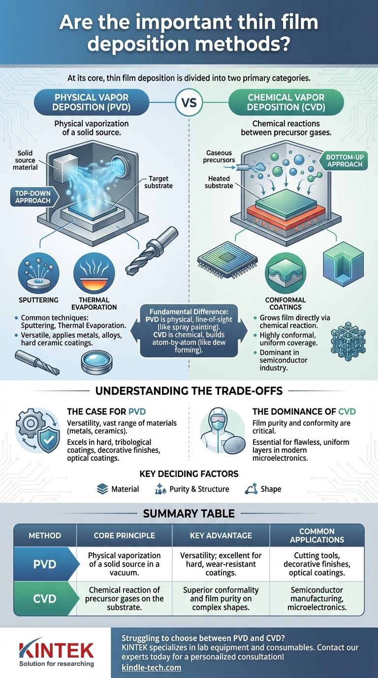
At its core, thin film deposition is divided into two primary categories. These foundational techniques are Physical Vapor Deposition (PVD) and Chemical Vapor Deposition (CVD). PVD involves physically vaporizing a solid source material in a vacuum and depositing it onto a surface, while CVD uses chemical reactions between precursor gases to grow a film directly on the substrate.
The fundamental difference lies in how the material travels to the surface. PVD is a physical, line-of-sight process akin to spray painting, whereas CVD is a chemical process that builds the film atom-by-atom, much like dew forming uniformly on a surface.
Deconstructing the Core Methods
Thin film deposition is the process of applying a very thin layer of material, from nanometers to micrometers thick, onto a surface or "substrate." This imparts new properties—such as wear resistance, optical reflection, or electrical conductivity—that the substrate material does not possess on its own.
Physical Vapor Deposition (PVD)
PVD encompasses a set of vacuum deposition methods that use physical processes to produce a vapor of material, which then condenses on the object to be coated.
Think of this as a "top-down" approach. You start with a solid block of the coating material, turn it into a vapor, and transport that vapor onto your target.
Common PVD techniques include sputtering and thermal evaporation. These methods are highly versatile and widely used for applying metals, alloys, and hard ceramic coatings.
Chemical Vapor Deposition (CVD)
CVD involves introducing volatile precursor gases into a chamber. These gases then react or decompose on the substrate's surface to produce the desired high-purity, high-performance thin film.
This is a "bottom-up" approach. The film is built directly on the surface through a chemical reaction, not by transporting an existing solid.
Because it relies on a chemical reaction rather than a line-of-sight path, CVD is exceptional at creating highly conformal coatings that uniformly cover even complex, non-flat surfaces. This precision makes it the dominant method in the semiconductor industry.
Understanding the Trade-offs
The choice between PVD and CVD is not about which is "better" overall, but which is the correct tool for a specific engineering goal. The decision hinges on the desired film properties, the substrate material, and the geometry of the part being coated.
The Case for PVD
PVD processes are often chosen for their versatility and ability to deposit a vast range of materials, including metals and ceramics that are difficult to produce as precursor gases for CVD.
It excels in applications like creating hard, tribological coatings for cutting tools, durable decorative finishes on consumer products, and optical coatings for lenses and mirrors.
The Dominance of CVD
CVD is the undisputed leader where film purity and conformity are the most critical requirements. Its ability to grow flawless, uniform layers is essential for building the intricate, multi-layered structures found in modern microelectronics.
It is the cornerstone of semiconductor manufacturing, used to create the high-purity silicon, silicon dioxide, and other layers that form transistors and integrated circuits.
Key Deciding Factors
The decision typically comes down to three factors: the material you need to deposit, the required purity and structure of the final film, and the shape of the object you are coating. If the goal is a pure, uniform layer on a complex shape, CVD is often the superior choice. If the goal is a hard, wear-resistant metallic coating, PVD is the standard.
Making the Right Choice for Your Application
Selecting the correct deposition method requires a clear understanding of your primary technical objective.
- If your primary focus is creating high-purity, defect-free layers for electronics: CVD is the industry-standard method due to its unparalleled precision and control.
- If your primary focus is enhancing the surface properties of a tool or component with a hard coating: PVD techniques like sputtering are the most direct and effective solution.
- If your primary focus is uniformly coating a complex, three-dimensional object: CVD's chemical, non-line-of-sight nature provides superior conformal coverage.
Ultimately, choosing the right deposition method is about controlling matter at the atomic scale to achieve a specific engineering outcome.
Summary Table:
| Method | Core Principle | Key Advantage | Common Applications |
|---|---|---|---|
| PVD (Physical Vapor Deposition) | Physical vaporization of a solid source in a vacuum | Versatility; excellent for hard, wear-resistant coatings | Cutting tools, decorative finishes, optical coatings |
| CVD (Chemical Vapor Deposition) | Chemical reaction of precursor gases on the substrate | Superior conformality and film purity on complex shapes | Semiconductor manufacturing, microelectronics |
Struggling to choose between PVD and CVD for your project? The right deposition method is critical to your success. KINTEK specializes in lab equipment and consumables, serving laboratory needs with expert advice and reliable solutions. Our team can help you select the perfect system to achieve the precise film properties your application demands, ensuring optimal performance and efficiency.
Contact our experts today for a personalized consultation!
Visual Guide
Related Products
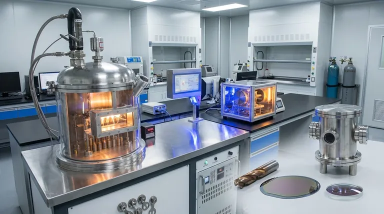
- Aluminized Ceramic Evaporation Boat for Thin Film Deposition
- Tungsten Evaporation Boat for Thin Film Deposition
- Electron Beam Evaporation Coating Oxygen-Free Copper Crucible and Evaporation Boat
- Molybdenum Tungsten Tantalum Evaporation Boat for High Temperature Applications
- Vacuum Hot Press Furnace Machine for Lamination and Heating
People Also Ask
- What is the chemical method for thin film deposition? Build Films from the Molecular Level Up
- What is the widely used boat made of in thermal evaporation? Choosing the Right Material for High-Purity Deposition
- Why is an alumina boat selected for catalyst precursors? Ensure Sample Purity at 1000 °C
- What are the alternatives to sputtering? Choose the Right Thin Film Deposition Method
- Why are high-purity ceramic boats used for lignin activation? Ensure Purity & Thermal Stability


