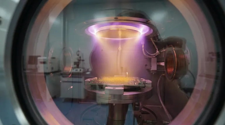
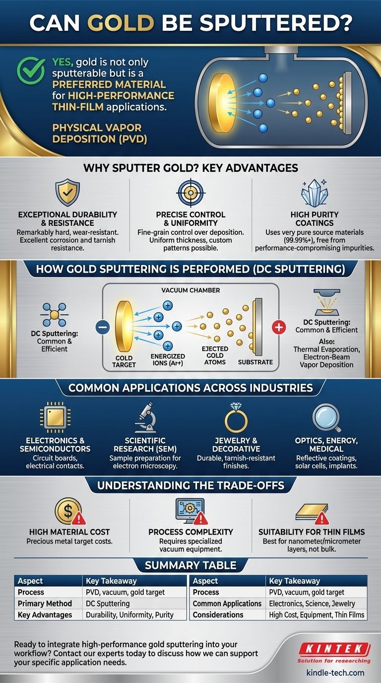
Yes, gold is not only sputterable but is a preferred material for high-performance thin-film applications. Sputtering is a physical vapor deposition (PVD) technique where a high-purity gold "target" is bombarded with energized ions in a vacuum. This process ejects individual gold atoms, which then travel and condense onto a component (the "substrate"), forming an exceptionally uniform, durable, and thin gold coating.
Gold sputtering is a standard industrial process used to create high-quality, functional gold films. The core value lies in its ability to produce coatings that are not just decorative but also highly durable, corrosion-resistant, and precisely controlled for technical applications.
Why Sputter Gold? The Key Advantages
The choice to sputter gold is driven by the unique properties of the resulting thin film, which often surpass those achieved through other coating methods.
Exceptional Durability and Resistance
Sputtered gold films are remarkably hard and wear-resistant. They do not easily rub off from contact with skin or clothing.
This durability is matched by excellent corrosion and tarnish resistance, ensuring the coating maintains its integrity and appearance even in demanding environments.
Precise Control and Uniformity
The sputtering process allows for fine-grain control over the deposition. Technicians can ensure a perfectly uniform coating thickness across complex surfaces.
This control also extends to creating custom patterns or even specific shades, such as rose gold, by introducing other elements into the process.
High Purity Coatings
Sputtering relies on very pure source materials, often exceeding 99.99% purity. This ensures that the final coating is free from impurities that could compromise its performance, a critical factor in electronics and scientific applications.
How Gold Sputtering is Performed
While the concept is straightforward, the execution is a precise technical process that falls under the category of Physical Vapor Deposition (PVD).
The Core Sputtering Process
Inside a vacuum chamber, a high-purity gold target is bombarded with energized ions, typically from an inert gas like argon. This high-energy impact dislodges, or "sputters," gold atoms from the target.
These ejected atoms then travel through the vacuum and deposit onto the substrate, building up a thin film atom by atom.
DC Sputtering: The Common Method
The most common technique for sputtering gold is Direct Current (DC) sputtering. Because gold is an excellent electrical conductor, a simple and cost-effective DC power source can be used to generate the plasma needed to bombard the target.
Alternative Deposition Techniques
While DC sputtering is the primary method, similar thin-film results can be achieved with other PVD processes. These include thermal evaporation, where gold is heated until it evaporates, and electron-beam vapor deposition, where a powerful electron beam is used to vaporize the gold source.
Common Applications Across Industries
Gold sputtering is not limited to a single field; its unique combination of properties makes it essential in numerous high-value sectors.
Electronics and Semiconductors
This is one of the largest applications. Gold's high conductivity and resistance to corrosion make it ideal for coating circuit boards, electrical contacts, and other critical electronic components.
Scientific Research
In Scanning Electron Microscopy (SEM), non-conductive samples must be coated with a conductive material to be imaged properly. Sputtering a micro-thin layer of gold is a standard procedure to prepare these specimens.
Jewelry and Decorative Finishes
For luxury goods like watches and rings, gold sputtering provides a durable and long-lasting finish that resists tarnishing and wear from daily use, far better than traditional plating.
Optics, Energy, and Medical
Gold's properties are also leveraged for specialized applications like creating reflective coatings for optical devices, improving efficiency in solar cells, and providing biocompatible, inert coatings for medical implants.
Understanding the Trade-offs
While highly effective, gold sputtering involves practical considerations that make it suitable for specific use cases.
High Material Cost
Gold is a precious metal, and the high-purity targets required for sputtering are a significant cost driver. The process is highly efficient with material, but the initial investment in the gold itself is high.
Process Complexity
Sputtering is not a simple benchtop process. It requires a vacuum chamber, high-voltage power supplies, and precise controls, making the equipment a considerable capital expense.
Suitability for Thin Films
Sputtering is fundamentally designed to create thin films, typically measured in nanometers or micrometers. It is not an effective or economical method for creating thick, bulk layers of gold.
Making the Right Choice for Your Goal
Deciding if gold sputtering is appropriate depends entirely on the required outcome.
- If your primary focus is functional electronics: Gold sputtering provides superior conductivity and corrosion resistance for critical components where reliability is essential.
- If your primary focus is high-end decorative finishes: The process creates a durable, tarnish-resistant, and premium coating for luxury goods that must withstand wear.
- If your primary focus is scientific sample preparation: Sputtering is the standard method for making non-conductive specimens visible and stable under an electron microscope.
Ultimately, gold sputtering is the definitive method for applying a high-performance, precision gold film where durability and reliability are paramount.
Summary Table:
| Aspect | Key Takeaway |
|---|---|
| Process | Physical Vapor Deposition (PVD) using a high-purity gold target in a vacuum. |
| Primary Method | DC Sputtering, ideal due to gold's high electrical conductivity. |
| Key Advantages | Exceptional durability, corrosion resistance, precise thickness control, and high purity. |
| Common Applications | Electronics/Semiconductors, Scientific Research (SEM), Jewelry, Medical Devices. |
| Considerations | High material cost, requires specialized vacuum equipment, suitable for thin films only. |
Ready to integrate high-performance gold sputtering into your workflow?
KINTEK specializes in providing the precise lab equipment and consumables needed for reliable Physical Vapor Deposition. Whether you are developing advanced electronics, preparing research samples, or creating durable decorative finishes, our solutions ensure the quality and consistency your projects demand.
Contact our experts today to discuss how we can support your specific application needs.
Visual Guide
Related Products
- Electron Beam Evaporation Coating Gold Plating Tungsten Molybdenum Crucible for Evaporation
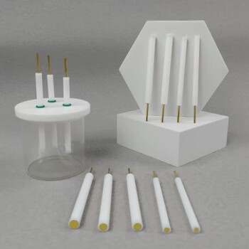
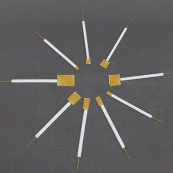
- Gold Disc Electrode
- Gold Electrochemical Sheet Electrode Gold Electrode
- Spark Plasma Sintering Furnace SPS Furnace
People Also Ask
- What is the current of e-beam evaporation? A Guide to High-Purity Thin Film Deposition
- How is an electron beam evaporator cooled during deposition? Essential Thermal Management for Stable Processes
- What is the process of e-beam coating? Achieve High-Purity, Precise Thin Films for Your Lab
- What materials are used in electron beam evaporation? Master High-Purity Thin Film Deposition
- What is the voltage of e-beam evaporation? Achieve Precise Thin-Film Deposition