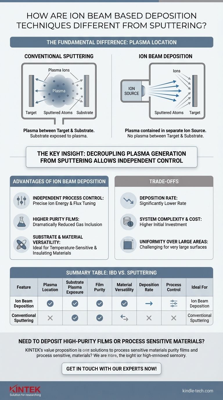
The fundamental difference between ion beam deposition and conventional sputtering lies in the location of the plasma. In conventional magnetron sputtering, a plasma is created and sustained in the space directly between the material source (the target) and the object being coated (the substrate). In stark contrast, ion beam deposition generates its plasma within a separate, contained ion source, which then directs a controlled beam of ions at the target. This deliberate separation of the plasma source from the deposition environment is the defining feature that unlocks a higher degree of process control.
The key insight is that by separating the ion source from the target and substrate, ion beam deposition decouples plasma generation from the sputtering process. This allows for independent control over ion energy and flux, resulting in higher-purity films and the ability to process sensitive or non-conductive materials that are incompatible with conventional sputtering methods.
The Core Mechanic: Plasma Location is Everything
To understand the practical implications of these two techniques, we must first examine how each one works at a fundamental level. The core distinction dictates the entire environment in which the thin film is grown.
How Conventional Sputtering Works
In a typical magnetron sputtering system, the chamber is filled with an inert gas, like Argon. A strong electric and magnetic field is applied between the target and substrate, which ignites and confines a plasma in this space.
Positively charged Argon ions from this plasma are accelerated into the negatively charged target. This high-energy bombardment physically ejects, or "sputters," atoms from the target material, which then travel through the plasma and deposit onto the substrate as a thin film. The substrate is continuously exposed to this plasma environment.
How Ion Beam Sputter Deposition (IBSD) Works
Ion beam sputter deposition completely re-architects this process. The plasma is created and contained entirely within a separate piece of hardware called an ion source.
This source extracts ions from its internal plasma and accelerates them as a well-defined, focused beam. This beam travels through a high-vacuum chamber and strikes the target. The sputtered atoms then travel unimpeded to the substrate. Critically, there is no plasma between the target and the substrate.
The Critical Separation
This separation is the source of nearly all of IBSD's advantages. The substrate is never exposed to the plasma, only to the flow of neutral atoms being sputtered from the target. This creates a much cleaner and more controlled environment for film growth.
Key Advantages of Ion Beam Deposition
The control afforded by separating the ion source from the deposition chamber provides several distinct benefits over conventional sputtering.
Independent Process Control
Because the ion source is an independent module, you can precisely and separately control the ion energy (beam voltage) and the ion flux (beam current). This allows for meticulous fine-tuning of the energy delivered to the target, which directly influences the properties of the resulting film, such as its density, stress, and stoichiometry.
Higher Purity Films
In magnetron sputtering, the substrate is bathed in the high-pressure inert gas plasma. This inevitably leads to some of the sputter gas becoming embedded, or "included," in the growing film. Since IBSD operates in a higher vacuum with no plasma near the substrate, sputter gas inclusion is dramatically reduced, resulting in purer, higher-quality films.
Substrate and Material Versatility
The lack of direct plasma exposure makes IBSD ideal for coating temperature-sensitive substrates, like polymers, that could be damaged by plasma heating. Furthermore, since the target does not need an electrical bias to sustain a plasma, IBSD works equally well for both conducting and non-conducting (insulating) target materials, a significant advantage over standard DC magnetron sputtering.
Understanding the Trade-offs
No technique is superior in all situations. Choosing between these methods requires acknowledging their practical limitations.
Deposition Rate
The primary advantage of magnetron sputtering is its significantly higher deposition rate. The dense plasma and proximity of the target allow for much faster film growth, making it the preferred method for high-throughput industrial manufacturing where speed is paramount.
System Complexity and Cost
Ion beam systems are inherently more complex. They require a sophisticated and expensive ion source, along with the associated power supplies and control electronics. This leads to a higher initial equipment cost and potentially more complex maintenance compared to simpler magnetron sputtering setups.
Uniformity Over Large Areas
While IBSD offers exceptional control, achieving highly uniform coatings over very large substrate areas can be more challenging than with well-designed magnetron sputtering systems. Sputtering from a large planar magnetron target is often a more direct path to achieving large-area uniformity.
Making the Right Choice for Your Application
The decision to use ion beam deposition or conventional sputtering is driven entirely by the priorities of your specific project.
- If your primary focus is high-throughput production and cost-efficiency: Conventional magnetron sputtering is almost always the superior choice due to its higher deposition rates and lower system complexity.
- If your primary focus is creating high-purity, dense films with precise control over properties: Ion beam sputter deposition is the definitive choice, especially for advanced optical coatings, sensitive substrates, or research applications.
- If your primary focus is depositing from insulating or dielectric target materials: Ion beam deposition provides a robust solution, although RF magnetron sputtering is also a common alternative to consider.
Ultimately, selecting the right technique requires aligning the unparalleled control of ion beam methods with the specific quality, material, and throughput demands of your project.
Summary Table:
| Feature | Ion Beam Deposition | Conventional Sputtering |
|---|---|---|
| Plasma Location | Separate ion source | Between target & substrate |
| Substrate Plasma Exposure | No | Yes |
| Film Purity | High (low gas inclusion) | Moderate (gas inclusion) |
| Material Versatility | Conductors & insulators | Primarily conductors (DC) |
| Deposition Rate | Lower | Higher |
| Process Control | Independent ion energy/flux | Coupled parameters |
| Ideal For | High-purity films, sensitive substrates | High-throughput production |
Need to deposit high-purity films or process sensitive materials?
KINTEK specializes in advanced lab equipment, including ion beam and sputtering systems, to meet your specific deposition challenges. Our expertise ensures you get the right solution for superior film quality, whether for research or production.
Contact us today to discuss your project and discover how our tailored solutions can enhance your laboratory's capabilities.
Get in touch with our experts now!
Visual Guide
Related Products
- Electron Beam Evaporation Coating Oxygen-Free Copper Crucible and Evaporation Boat
- Electron Beam Evaporation Coating Tungsten Crucible and Molybdenum Crucible for High Temperature Applications
- Molybdenum Tungsten Tantalum Evaporation Boat for High Temperature Applications
- Electron Beam Evaporation Coating Gold Plating Tungsten Molybdenum Crucible for Evaporation
- Electron Beam Evaporation Coating Conductive Boron Nitride Crucible BN Crucible
People Also Ask
- What is e-beam evaporation used for? Precision Coating for Optics, Aerospace & Electronics
- How is an electron beam evaporator cooled during deposition? Essential Thermal Management for Stable Processes
- What is the container that holds the metal source material called in e-beam evaporation? Ensure Purity and Quality in Your Thin-Film Deposition
- What is the current of e-beam evaporation? A Guide to High-Purity Thin Film Deposition
- What is the temperature of e-beam evaporation? Mastering the Two-Zone Thermal Process for Precision Films


