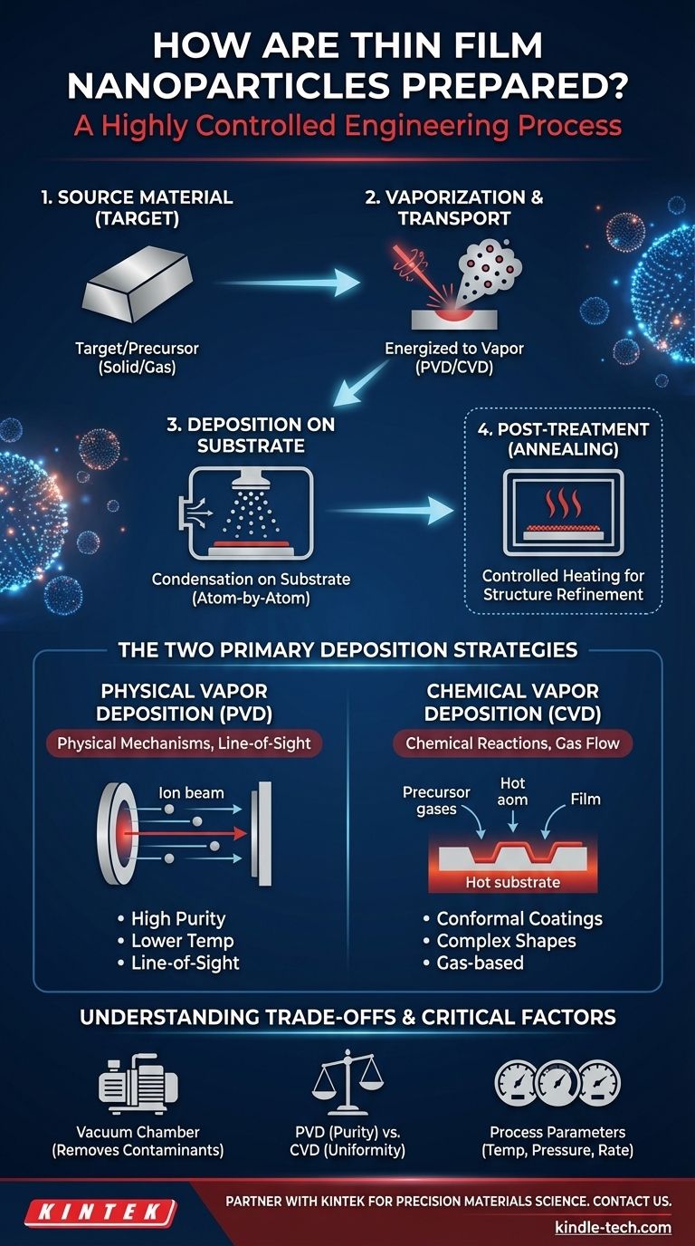
At its core, preparing thin film nanoparticles is a highly controlled, three-stage process. It begins with a source material, known as a target, which is energized within a vacuum chamber until it vaporizes. This vapor is then transported and allowed to condense onto a surface, called a substrate, forming an ultra-thin layer. Finally, this newly formed film may undergo a heat treatment process, or annealing, to refine its final structure and properties.
The creation of nanoparticle thin films is not simply a coating process; it is a precisely controlled engineering task. The goal is to manipulate material in a gaseous or plasma state to build a solid film with specific nanoscale properties, a process fundamentally divided into physical and chemical methods.
The Foundational Steps of Thin Film Deposition
Every thin film preparation method, regardless of its specific technology, follows a logical sequence of events. Understanding this universal workflow is the first step to mastering the technique.
Step 1: Selecting the Source Material (The "Target")
The process begins with the raw material you intend to deposit. This is called the target or precursor.
The form of this source material depends entirely on the chosen deposition technique. It can be a solid block of high-purity metal, a ceramic puck, or a specialized reactive gas.
Step 2: Energizing and Transporting the Material
This is the most critical stage and where different techniques diverge significantly. The goal is to convert the source material into a vapor that can travel to the substrate.
This is achieved by adding energy. Methods can include heating the material until it evaporates, bombarding it with ions to physically knock atoms loose (sputtering), or introducing precursor gases that will later react chemically.
Step 3: Deposition onto the Substrate
Within the vacuum chamber, the vaporized material travels until it strikes the substrate, which is the object or surface being coated.
Upon hitting the cooler substrate surface, the atoms or molecules lose energy and condense, forming a solid layer. This film builds up atom-by-atom, creating a tightly controlled nanostructure.
Step 4: Post-Deposition Treatment (Annealing)
In many cases, the film as-deposited is not in its final, optimal state.
Annealing, a carefully controlled heat treatment process, is often used to improve the film's crystallinity, reduce internal stresses, and enhance its electronic or optical properties.
The Two Primary Deposition Strategies
While the steps are similar, the methods for executing them fall into two major families: Physical Vapor Deposition (PVD) and Chemical Vapor Deposition (CVD).
Physical Vapor Deposition (PVD)
PVD uses purely physical mechanisms to generate the material vapor. Think of it as a microscopic sandblasting process.
An energy source (like an ion beam) strikes the solid target, physically dislodging atoms or molecules that then travel in a straight line to coat the substrate. This is a line-of-sight process.
Chemical Vapor Deposition (CVD)
CVD uses chemical reactions to form the film. Precursor gases are introduced into the vacuum chamber.
These gases react on the hot substrate surface, leaving behind the desired solid material as a byproduct and forming a film. Because it relies on gas flow, CVD can effectively coat complex, non-flat surfaces.
Understanding the Trade-offs
Choosing the right method requires understanding the inherent limitations and requirements of the deposition environment.
The Critical Role of the Vacuum
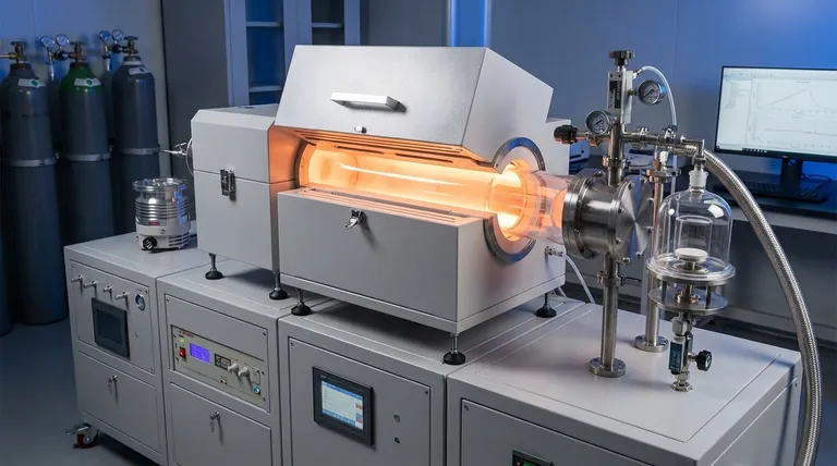
Nearly all thin film deposition is performed in a vacuum chamber. This is non-negotiable for high-quality films.
The vacuum removes air and other contaminants that could otherwise react with the vaporized material, introducing impurities into the film and compromising its properties.
PVD vs. CVD Considerations
PVD is often chosen for its ability to deposit extremely high-purity materials, including metals and ceramics, at lower temperatures than many CVD processes.
CVD excels at creating uniform, conformal coatings over intricate 3D geometries, something that is difficult for line-of-sight PVD techniques.
Process Parameters are Key
The final properties of the nanoparticle film are not just determined by the material. They are a direct result of process parameters like pressure, temperature, and deposition rate. Precise control over these variables is essential to achieving the desired outcome.
Making the Right Choice for Your Goal
Your application dictates the ideal deposition strategy. Use your end-goal to guide your decision.
- If your primary focus is high-purity metallic or optical films: PVD methods like sputtering or thermal evaporation provide exceptional control over film composition and purity.
- If your primary focus is uniform coating on complex shapes: CVD is generally more effective due to its non-line-of-sight, gas-based deposition mechanism.
- If your primary focus is a specific crystalline structure: Post-deposition annealing is a critical and independent process step that you must plan for and optimize.
Understanding these fundamental principles empowers you to select and control the deposition process to engineer thin films with precisely tailored nanoparticle properties.
Summary Table:
| Key Stage | Primary Goal | Common Methods |
|---|---|---|
| 1. Source Preparation | Provide high-purity material | Solid target (PVD), Precursor gas (CVD) |
| 2. Vaporization & Transport | Energize material into a vapor | Sputtering, Evaporation (PVD), Gas reaction (CVD) |
| 3. Deposition | Condense vapor onto substrate | Line-of-sight condensation (PVD), Surface reaction (CVD) |
| 4. Post-Treatment (Annealing) | Improve film structure & properties | Controlled heat treatment |
Ready to Engineer Your Next Generation of Materials?
Precision is paramount in thin film deposition. The quality of your film directly depends on the reliability of your equipment and consumables. KINTEK specializes in high-purity lab equipment and consumables—from sputtering targets and CVD precursors to vacuum components and annealing furnaces—serving the exacting needs of materials science and R&D laboratories.
Let us help you achieve the precise control required for your specific application. Contact our experts today to discuss your project requirements and discover how KINTEK can support your innovation.
Visual Guide
Related Products
- Aluminized Ceramic Evaporation Boat for Thin Film Deposition
- Electron Beam Evaporation Coating Oxygen-Free Copper Crucible and Evaporation Boat
People Also Ask
- What are thin films deposited by evaporation? A Guide to High-Purity Coating
- Why is an alumina boat selected for catalyst precursors? Ensure Sample Purity at 1000 °C
- Why are high-purity ceramic boats used for lignin activation? Ensure Purity & Thermal Stability
- What is the chemical method for thin film deposition? Build Films from the Molecular Level Up
- Why is an alumina boat and Ti3AlC2 powder bed necessary for Ti2AlC sintering? Protect MAX Phase Purity

