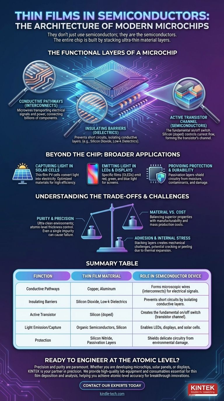
In essence, thin films are not just used in semiconductors; they are the semiconductors. The entire architecture of a modern microchip, from its wires to its switches, is built by meticulously depositing and etching a sequence of these ultra-thin material layers. They perform every critical function, serving as conductive, insulating, and active semiconducting layers to create complex integrated circuits.
The core principle to understand is that semiconductor manufacturing is fundamentally the art of stacking and patterning thin films. Each film is a distinct layer, often just atoms thick, with a specific electrical or physical job—conducting current, blocking it, or switching it on and off—which together form the billions of transistors powering our devices.
The Functional Layers of a Microchip
To understand how thin films work in semiconductors, it's best to think of them by the distinct role each layer plays. A modern processor is a three-dimensional city of circuits built layer by layer.
As Conductive Pathways (Interconnects)
The transistors on a chip must be wired together. This is accomplished by depositing a thin film of a conductive metal, typically copper or aluminum.
These metallic films act as the microscopic "wires" and "highways" that transport electrical signals and power throughout the integrated circuit, connecting billions of individual components.
As Insulating Barriers (Dielectrics)
To prevent the immense network of conductive pathways from short-circuiting, they must be electrically isolated from one another. This is the job of dielectric thin films.
Materials like silicon dioxide or more advanced "low-k" dielectrics are deposited between the conductive layers. They act as insulators, ensuring that electrical signals stay in their designated paths.
As the Active Transistor Channel (Semiconductors)
This is the heart of the device. The active, switching part of a transistor is itself made from a thin film of semiconductor material, most commonly silicon.
By introducing impurities into the silicon film in a process called doping, engineers create regions that form the transistor's gate, source, and drain. Applying a voltage to the gate's thin film controls the flow of current through the channel, creating the fundamental on/off switch of digital logic.
Beyond the Chip: Broader Semiconductor Applications
The same principles of using thin films to control electrons and light extend to many other semiconductor devices beyond microprocessors.
Capturing Light in Solar Cells
Thin-film photovoltaic cells are a prime example. Layers of semiconductor materials are deposited onto a substrate like glass or plastic.
When light strikes these films, it excites electrons, generating an electrical current. The choice of material and the thickness of the films are optimized to capture the maximum amount of light energy.
Emitting Light in LEDs and Displays
In Organic Light Emitting Diodes (OLEDs) and other modern displays, specific thin films are chosen for their ability to emit light when electricity passes through them.
By stacking different organic or semiconductor films, manufacturers can produce the red, green, and blue light needed to create vibrant, full-color images on our phone and TV screens.
Providing Protection and Durability
Finally, the finished semiconductor device is often coated with a protective thin film. This final layer, known as a passivation layer, shields the delicate internal circuitry from moisture, contaminants, and physical damage, ensuring reliability and longevity.
Understanding the Trade-offs and Challenges
The precision required in thin film deposition is staggering, and every choice involves significant engineering trade-offs.
The Challenge of Purity and Precision
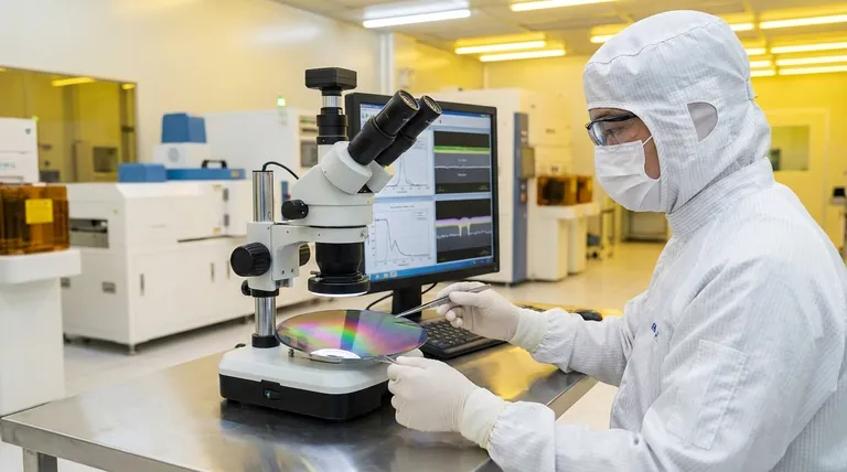
The deposition process, whether physical (PVD) or chemical (CVD), must be executed in an ultra-clean environment. A single microscopic dust particle or atomic impurity in a film can render a billion-dollar chip useless.
The thickness of each layer must be controlled with atomic-level accuracy to ensure the device performs as designed.
Material Properties vs. Cost
The choice of material for each film is a constant balance. An exotic metal might offer superior conductivity, but its cost or difficulty of deposition could make it impractical for mass production.
Engineers must constantly weigh the performance benefits of a material against its manufacturability and cost, especially for consumer electronics or large-area devices like solar panels.
Adhesion and Internal Stress
Stacking dozens or even hundreds of different material layers creates immense mechanical challenges. Each film must adhere perfectly to the one below it.
Furthermore, differences in how materials expand and contract with heat can create internal stress, potentially causing layers to crack or peel apart, leading to device failure.
How to Apply This to Your Goal
Your focus dictates which aspect of thin film technology is most critical.
- If your primary focus is computational performance (CPUs, GPUs): The key is using ultra-pure silicon films and advanced, low-k dielectric materials to pack more transistors into a smaller space and run them faster.
- If your primary focus is energy generation (Solar Panels): The priority is developing thin film materials with high photovoltaic efficiency that can be deposited cheaply over very large areas.
- If your primary focus is display technology (OLEDs): The goal is to engineer novel organic thin films that produce bright, efficient light and can be applied to flexible substrates.
- If your primary focus is device reliability and durability: You will concentrate on the properties of passivation layers and protective coatings that resist corrosion, wear, and environmental stress.
Ultimately, mastering thin film technology is mastering the ability to engineer matter at the atomic scale, a skill that underpins the entire digital world.
Summary Table:
| Function | Thin Film Material | Role in Semiconductor Device |
|---|---|---|
| Conductive Pathways | Copper, Aluminum | Forms microscopic wires (interconnects) for electrical signals. |
| Insulating Barriers | Silicon Dioxide, Low-k Dielectrics | Prevents short circuits by isolating conductive layers. |
| Active Transistor | Silicon (doped) | Creates the fundamental on/off switch (transistor channel). |
| Light Emission/Capture | Organic Semiconductors, Silicon | Enables LEDs, displays, and solar cells. |
| Protection | Silicon Nitride, Passivation Layers | Shields delicate circuitry from environmental damage. |
Ready to Engineer at the Atomic Level?
The precision and purity of your thin films are paramount to your device's performance. Whether you are developing advanced microchips, high-efficiency solar panels, or next-generation displays, KINTEK is your partner in precision.
We specialize in providing the high-quality lab equipment and consumables essential for research, development, and quality control in thin film deposition and analysis. Our solutions help you achieve the atomic-level accuracy required for breakthrough innovations.
Contact our experts today to discuss how we can support your specific semiconductor or advanced materials project. Let's build the future, together.
Visual Guide
Related Products
- Aluminized Ceramic Evaporation Boat for Thin Film Deposition
- Tungsten Evaporation Boat for Thin Film Deposition
- Electron Beam Evaporation Coating Oxygen-Free Copper Crucible and Evaporation Boat
- Molybdenum Tungsten Tantalum Evaporation Boat for High Temperature Applications
- HFCVD Machine System Equipment for Drawing Die Nano-Diamond Coating
People Also Ask
- What are thin films deposited by evaporation? A Guide to High-Purity Coating
- What is the chemical method for thin film deposition? Build Films from the Molecular Level Up
- What are the alternatives to sputtering? Choose the Right Thin Film Deposition Method
- What is thin film deposition? Unlock Advanced Surface Engineering for Your Materials
- What is the source of evaporation for thin film? Choosing Between Thermal and E-Beam Methods


