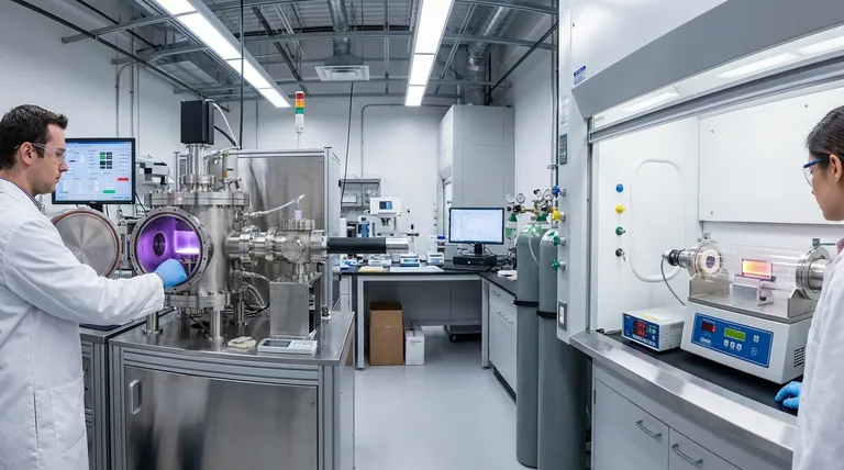
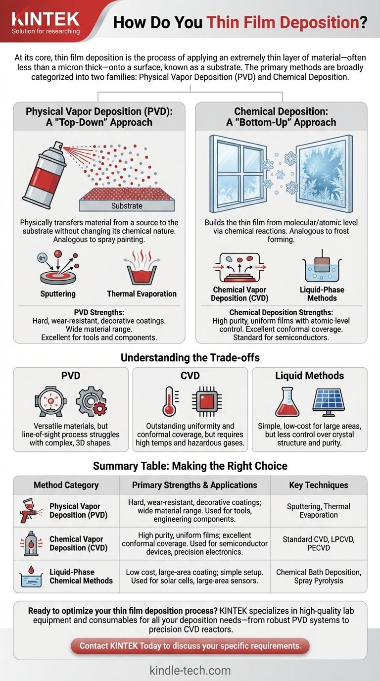
At its core, thin film deposition is the process of applying an extremely thin layer of material—often less than a micron thick—onto a surface, known as a substrate. The primary methods for achieving this are broadly categorized into two families: Physical Vapor Deposition (PVD), which physically transfers material from a source to the substrate, and Chemical Deposition, where chemical reactions form the film directly on the substrate's surface.
The fundamental choice in thin film deposition is not about which method is "best," but which process—physical transfer or chemical reaction—provides the specific film properties, purity, and precision your application demands.
The Core Principles: Physical vs. Chemical Deposition
To understand how thin films are deposited, you must first grasp the two fundamentally different philosophies behind the main techniques. One is analogous to spray painting, while the other is more like frost forming on a window.
Physical Vapor Deposition (PVD): A "Top-Down" Approach
PVD is a process that takes a solid source material, vaporizes it in a vacuum, and then deposits it onto the substrate. The material is physically moved from the source to the target without changing its chemical nature.
Common PVD techniques include sputtering, where high-energy ions bombard the source material to eject atoms, and thermal evaporation, which uses heat to turn the source material into a vapor.
Chemical Deposition: A "Bottom-Up" Approach
Chemical deposition methods build the thin film from the molecular or atomic level through chemical reactions. This allows for the creation of highly pure and complex material layers.
This category is further divided. The most prominent method is Chemical Vapor Deposition (CVD), which uses precursor gases that react or decompose on the substrate surface to form the desired film. Other methods, often called liquid-phase techniques, use chemical solutions.
A Closer Look at Deposition Techniques
While PVD and CVD are the dominant methods, especially in high-tech fields, several specific techniques exist within each category. Each is suited for different materials and outcomes.
PVD in Practice: Coating for Durability
PVD is highly versatile and is often used to deposit coatings that improve the mechanical properties of a surface. This includes metals, alloys, and certain compounds.
Because it's a direct line-of-sight physical process, PVD is excellent for creating hard, wear-resistant, or corrosion-resistant layers on engineering components like tools and machine parts.
CVD in Practice: Building with Precision
CVD is the cornerstone of the semiconductor industry. Its ability to grow exceptionally uniform and high-purity films with atomic-level control is critical for manufacturing integrated circuits.
The process involves carefully controlled temperature, pressure, and gas flow, allowing for the precise deposition of materials essential for modern electronics.
Liquid-Phase Methods: Simplicity and Scale
Simpler chemical methods that don't require a vacuum are also common. These are often less precise but can be more cost-effective for certain applications.
Techniques include chemical bath deposition, where a substrate is simply submerged in a solution, and spray pyrolysis, which involves spraying a chemical solution onto a heated substrate to trigger a reaction.
Understanding the Trade-offs
Choosing a deposition method is a matter of balancing complexity, cost, and the required film characteristics. There is no single solution for every problem.
PVD: Versatility vs. Conformal Coverage
PVD can deposit a vast range of materials. However, because it's a line-of-sight process, it can struggle to evenly coat complex, three-dimensional shapes.
CVD: Precision vs. Process Conditions
CVD provides outstanding film uniformity and can coat complex shapes perfectly. However, it often requires very high temperatures and volatile, sometimes hazardous, precursor gases, making the process more complex and restrictive.
Liquid Methods: Cost-Effectiveness vs. Purity
Liquid-phase techniques are often the simplest and cheapest to implement, making them ideal for large-area coatings where ultimate purity is not the primary concern. The trade-off is typically less control over the film's crystal structure and purity compared to vacuum-based methods.
Making the Right Choice for Your Application
Your final decision must be guided by the intended function of the thin film.
- If your primary focus is high-purity, uniform electronic films: CVD is the industry standard due to its atomic-level precision and excellent conformal coverage.
- If your primary focus is applying hard, wear-resistant, or decorative coatings: PVD techniques offer unparalleled versatility for depositing a wide range of robust materials.
- If your primary focus is low-cost, large-area coating without vacuum: Liquid-phase chemical methods like spray pyrolysis or chemical bath deposition can be highly effective.
Ultimately, selecting the correct deposition method is about aligning the unique strengths of a process with the specific performance goals for your material.
Summary Table:
| Method Category | Key Technique | Primary Strengths | Common Applications |
|---|---|---|---|
| Physical Vapor Deposition (PVD) | Sputtering, Thermal Evaporation | Hard, wear-resistant coatings; wide material range | Tool coatings, decorative layers, engineering components |
| Chemical Vapor Deposition (CVD) | Standard CVD, LPCVD, PECVD | High purity, uniform films; excellent conformal coverage | Semiconductor devices, integrated circuits, precision electronics |
| Liquid-Phase Chemical Methods | Chemical Bath Deposition, Spray Pyrolysis | Low cost, large-area coating; simple setup | Solar cells, large-area sensors, cost-effective coatings |
Ready to optimize your thin film deposition process? The right equipment is critical for achieving the film purity, uniformity, and performance your application demands. At KINTEK, we specialize in providing high-quality lab equipment and consumables for all your deposition needs—from robust PVD systems for durable coatings to precision CVD reactors for semiconductor-grade films. Our experts can help you select the perfect solution to enhance your research or production. Contact our team today to discuss your specific requirements and discover how KINTEK can support your laboratory's success.
Visual Guide
Related Products
- Aluminized Ceramic Evaporation Boat for Thin Film Deposition
- Tungsten Evaporation Boat for Thin Film Deposition
- Electron Beam Evaporation Coating Oxygen-Free Copper Crucible and Evaporation Boat
- Molybdenum Tungsten Tantalum Evaporation Boat for High Temperature Applications
- HFCVD Machine System Equipment for Drawing Die Nano-Diamond Coating
People Also Ask
- What is the widely used boat made of in thermal evaporation? Choosing the Right Material for High-Purity Deposition
- Why is an alumina boat selected for catalyst precursors? Ensure Sample Purity at 1000 °C
- What is thin film deposition? Unlock Advanced Surface Engineering for Your Materials
- What are the alternatives to sputtering? Choose the Right Thin Film Deposition Method
- What are the applications of thin films deposition? Unlock New Possibilities for Your Materials


