A 13.56 MHz RF power supply facilitates film densification by applying a high-frequency electric field that ionizes reactive gases into plasma. This ionization process provides the energy necessary to activate chemical species within the reaction chamber. By controlling this energy, the system drives the structural changes required to create a dense organosilicon film.
The RF power supply acts as the primary control lever for film quality. It regulates the energy level of the plasma to induce molecular cross-linking, allowing you to achieve high film density without the risks associated with external heating.
The Mechanism of Plasma Generation
Creating the Electric Field
The power supply delivers high-frequency energy to the reaction chamber through an upper electrode.
This creates a pervasive electric field necessary to initiate the deposition process.
Ionization of Reactive Gases
Within this field, reactive gases are stripped of electrons and ionized.
This transition from gas to plasma creates a highly active environment filled with energetic species ready to react with the substrate.
Controlling Film Properties via Power Regulation
Tuning Excitation Power
Operators can precisely adjust the RF excitation power, typically within a range of 50 to 300 W.
This adjustment directly dictates the average energy and activation level of the plasma species.
Managing Monomer Fragmentation
The input power controls how monomer molecules are broken down (fragmented) within the chamber.
Precise fragmentation is the precursor to building a stable film structure.
Inducing Chain Segment Cross-Linking
The primary mechanism for densification is chain segment cross-linking.
The activated plasma species bond together tightly, compacting the film structure and increasing its density.
Critical Operational Considerations
The Non-Thermal Advantage
A significant advantage of this method is the ability to densify films without external heating.
The energy required for cross-linking comes solely from the RF-induced plasma, protecting temperature-sensitive substrates.
The Necessity of Balance
Achieving the correct density requires careful modulation of the activation level.
If the power is not optimized, the fragmentation and subsequent cross-linking may not occur efficiently enough to produce the desired film properties.
Optimizing Your Deposition Strategy
To leverage a 13.56 MHz RF power supply effectively, you must align the power settings with your specific film requirements.
- If your primary focus is Maximum Density: Increase the RF power within the 50-300 W range to maximize cross-linking and tighten the film structure.
- If your primary focus is Process Control: Use the power supply to fine-tune the fragmentation rate of monomers, ensuring consistent activation levels across the batch.
By mastering the correlation between RF power and plasma activation, you gain complete control over the structural integrity of your organosilicon films.
Summary Table:
| Feature | Description | Impact on Film |
|---|---|---|
| Frequency | 13.56 MHz | Efficient gas ionization and plasma stability |
| Power Range | 50 - 300 W | Controls average energy and activation levels |
| Mechanism | Chain Cross-linking | Increases film density and structural integrity |
| Thermal Load | Non-thermal | Protects temperature-sensitive substrates |
Elevate Your Thin Film Deposition with KINTEK
Maximize your research precision and film quality with KINTEK’s advanced laboratory solutions. Whether you are optimizing CVD and PECVD processes or developing next-generation materials, our high-performance 13.56 MHz RF power supplies and integrated vacuum systems provide the control you need for superior densification.
From high-temperature furnaces and vacuum reactors to specialized PTFE and ceramic consumables, KINTEK specializes in equipping world-class laboratories with reliable tools for battery research, material science, and thin-film engineering.
Ready to achieve high film density without compromising substrate integrity? Contact our technical experts today to find the perfect equipment for your specific application!
References
- Rita C. C. Rangel, Elidiane Cipriano Rangel. Role of the Plasma Activation Degree on Densification of Organosilicon Films. DOI: 10.3390/ma13010025
This article is also based on technical information from Kintek Solution Knowledge Base .
Related Products
- Reference Electrode Calomel Silver Chloride Mercury Sulfate for Laboratory Use
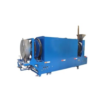
- RF PECVD System Radio Frequency Plasma-Enhanced Chemical Vapor Deposition RF PECVD
- Laboratory CVD Boron Doped Diamond Materials
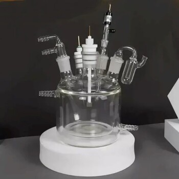
- Multifunctional Electrolytic Electrochemical Cell Water Bath Single Layer Double Layer
- 915MHz MPCVD Diamond Machine Microwave Plasma Chemical Vapor Deposition System Reactor
People Also Ask
- What is the purpose of the reference electrode? Achieve Stable & Accurate Electrochemical Measurements
- Which electrode is used as a ground reference? Master the Key to Accurate Electrochemical Measurements
- Why is the selection of a high-quality reference electrode critical in the electrochemical synthesis? | KINTEK
- What is the function of a reference electrode? Master Precision in Three-Electrode Reactor Reconstruction
- What is the reference electrode in potentiometry? The Key to Stable & Accurate Measurements