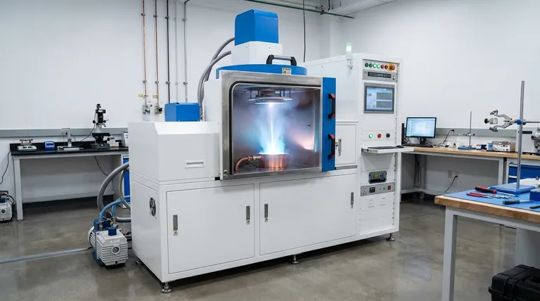
In short, electron beam evaporation is a process that uses a high-energy beam of electrons to boil a material inside a vacuum chamber. This creates a vapor of the source material, which then travels and condenses onto a target object, known as a substrate, forming an exceptionally pure and thin coating.
The core principle is not merely heating, but the precise and efficient transfer of energy. By converting the kinetic energy of electrons directly into thermal energy within the target material, this method bypasses many sources of contamination, making it a cornerstone technique for high-performance thin-film applications.
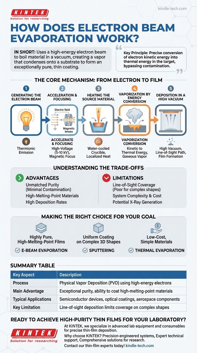
The Core Mechanism: From Electron to Film
Electron beam (e-beam) evaporation is a sophisticated form of Physical Vapor Deposition (PVD). Understanding its sequential steps reveals why it is so effective for creating high-quality films.
Step 1: Generating the Electron Beam
The process begins with a tungsten filament. A strong electric current passes through this filament, heating it to extreme temperatures.
This intense heat causes the filament to release a cloud of electrons through a process known as thermionic emission.
Step 2: Acceleration and Focusing
Once freed, these electrons are accelerated by a high-voltage electric field, typically between 5 and 10 kilovolts (kV), which gives them immense kinetic energy.
A magnetic system then focuses these high-speed electrons into a tight, controllable beam, much like a lens focuses light.
Step 3: Heating the Source Material
This focused beam is directed onto the source material (the "evaporant") that is to be deposited.
The material rests inside a water-cooled crucible, usually made of copper. This cooling is critical, as it ensures that the intense heat is localized only to the source material, preventing the crucible itself from melting or contaminating the process.
Step 4: Vaporization by Energy Conversion
Upon impact, the high kinetic energy of the electrons is instantly converted into thermal energy within the source material.
This rapid and concentrated heating causes the material to melt and then evaporate, turning directly into a gaseous vapor. This is far more efficient than heating the entire crucible.
Step 5: Deposition in a High Vacuum
The entire operation takes place inside a high vacuum chamber. This vacuum is essential to ensure the vaporized particles can travel unimpeded to the substrate without colliding with air molecules.
The vapor travels in a straight, line-of-sight path upwards, where it strikes the cooler substrate. Upon contact, the vapor condenses back into a solid, forming a thin, dense, and highly pure film on the substrate's surface.
Understanding the Trade-offs
While powerful, e-beam evaporation has specific characteristics that make it suitable for some applications but less ideal for others. Understanding these trade-offs is key to making an informed decision.
Advantage: Unmatched Purity and Material Range
Because the electron beam directly heats only the source material, contamination from the crucible is virtually eliminated. This results in films of exceptional purity.
This direct heating method also allows for the evaporation of materials with very high melting points, such as tungsten and tantalum, which are difficult or impossible to process with simpler thermal methods.
Advantage: High Deposition Rates
The energy transfer from the electron beam to the source material is extremely efficient. This allows for much higher deposition rates compared to other techniques like thermal evaporation or sputtering, enabling faster manufacturing.
Limitation: Line-of-Sight Coverage
The vapor travels in a straight line from the source to the substrate. This can be a problem when coating complex, three-dimensional objects, as surfaces not in the direct "line of sight" will receive little to no coating. This is known as poor "step coverage."
Limitation: System Complexity and X-Ray Generation
E-beam systems are more complex and expensive than simple resistive thermal evaporators due to the need for high-voltage power supplies and magnetic focusing systems.
Furthermore, the impact of high-energy electrons on the target material can generate X-rays. This may require shielding for safety and can potentially damage radiation-sensitive substrates or films.
Making the Right Choice for Your Goal
Selecting a deposition method depends entirely on your project's specific requirements for purity, material, geometry, and budget.
- If your primary focus is creating highly pure films of high-melting-point materials: E-beam evaporation is the superior choice due to its direct, efficient, and clean heating mechanism.
- If your primary focus is achieving a uniform coating on a complex 3D shape: A non-directional method like sputtering is likely a better option to ensure complete and even coverage.
- If your primary focus is low-cost deposition of simple, low-melting-point materials: A basic thermal evaporation system may be more than sufficient and far more cost-effective.
Ultimately, mastering thin-film deposition comes from matching the unique principles of the technique to the specific outcome you need to achieve.
Summary Table:
| Key Aspect | Description |
|---|---|
| Process | Physical Vapor Deposition (PVD) using high-energy electrons |
| Main Advantage | Exceptional purity and ability to coat high-melting-point materials |
| Typical Applications | Semiconductor devices, optical coatings, aerospace components |
| Key Limitation | Line-of-sight deposition limits coverage on complex shapes |
Ready to Achieve High-Purity Thin Films for Your Laboratory?
At KINTEK, we specialize in advanced lab equipment and consumables for precise thin-film deposition. Our electron beam evaporation systems are designed to help research and industrial laboratories create ultra-pure coatings with exceptional material compatibility.
Why choose KINTEK for your deposition needs?
- Precision-engineered systems for reliable, repeatable results
- Expert technical support for your specific application requirements
- Comprehensive solutions for semiconductor, optical, and materials research
Contact our thin-film experts today to discuss how our electron beam evaporation solutions can advance your research or production capabilities. Let us help you select the perfect system for your high-purity coating requirements.
Visual Guide
Related Products
- Electron Beam Evaporation Coating Tungsten Crucible and Molybdenum Crucible for High Temperature Applications
- Electron Beam Evaporation Coating Oxygen-Free Copper Crucible and Evaporation Boat
- Electron Beam Evaporation Coating Gold Plating Tungsten Molybdenum Crucible for Evaporation
- Electron Beam Evaporation Coating Conductive Boron Nitride Crucible BN Crucible
- E Beam Crucibles Electron Gun Beam Crucible for Evaporation
People Also Ask
- What is the voltage of e-beam evaporation? Achieve Precise Thin-Film Deposition
- What is e-beam evaporation? Achieve High-Purity Thin Film Deposition for Your Lab
- What is the temperature of e-beam evaporation? Mastering the Two-Zone Thermal Process for Precision Films
- What is the current of e-beam evaporation? A Guide to High-Purity Thin Film Deposition
- What materials are used in electron beam evaporation? Master High-Purity Thin Film Deposition


