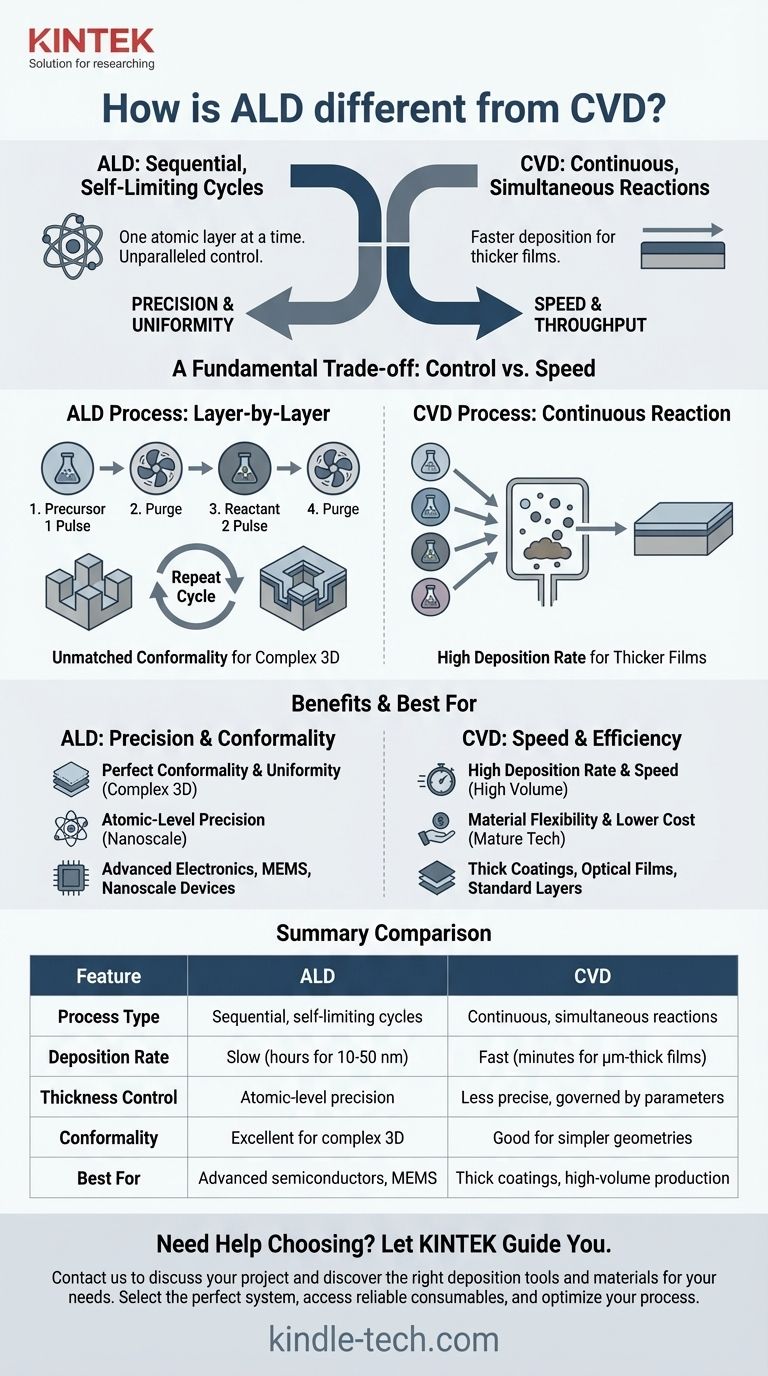
At their core, the fundamental difference between Atomic Layer Deposition (ALD) and Chemical Vapor Deposition (CVD) is the method of reaction. ALD is a sequential process that deposits material one single atomic layer at a time in self-limiting cycles, offering unparalleled control. In contrast, CVD involves continuous, simultaneous chemical reactions, enabling much faster deposition rates for thicker films.
Choosing between ALD and CVD is a fundamental trade-off between control and speed. ALD provides atomic-level precision and perfect uniformity, making it ideal for advanced, complex structures, while CVD provides the high-speed throughput necessary for thicker, less intricate coatings.
The Fundamental Process Distinction
To understand their different outcomes, we must first examine how each process works at a molecular level. Though both are forms of chemical vapor deposition, their execution is radically different.
ALD: The Layer-by-Layer Approach
Atomic Layer Deposition (ALD) separates the chemical reaction into two or more distinct, sequential steps. First, a precursor gas is pulsed into the chamber, where it forms a single, self-limiting monolayer on the substrate. This means the reaction stops automatically once all available surface sites are occupied.
Any excess precursor is purged, and then a second reactant is introduced. This second reactant interacts only with the first monolayer, completing the chemical reaction to form one atomic layer of the desired material. This cycle is repeated hundreds or thousands of times to build the film layer by layer.
CVD: The Continuous Reaction Approach
Chemical Vapor Deposition (CVD) takes a more direct route. In this process, all necessary precursor gases are introduced into the reaction chamber simultaneously.
These gases react together both on the substrate surface and in the volume above it, continuously depositing the material. The process is governed by factors like gas flow, temperature, and pressure, and it does not stop until the gases are shut off.
How Process Dictates Performance
The difference between a sequential, self-limiting process and a continuous one has profound implications for the final film's properties and the applications each technique is suited for.
Unmatched Conformality and Uniformity (ALD)
Because the ALD reaction is self-limiting, it can perfectly coat incredibly complex, three-dimensional structures with high aspect ratios. The film thickness will be identical on the top, sides, and bottom of any feature, a property known as high conformality.
This makes ALD essential for modern electronics, where features are nanoscale and three-dimensional. It excels at creating the very thin films (typically 10-50 nm) required for these applications.
Atomic-Level Thickness Control (ALD)
In ALD, the film thickness is determined simply by the number of reaction cycles performed. This direct relationship provides digital, atomic-level precision that is impossible to achieve with other methods.
Speed and Throughput (CVD)
The primary advantage of CVD is its high deposition rate. Because the reactions run continuously, it can deposit material much faster than ALD, making it far more economical for applications requiring thick films (hundreds of nanometers to several micrometers).
Material and Precursor Flexibility (CVD)
Historically, CVD has a broader library of established processes and available precursors for a wider range of materials. It is a mature, well-understood technology used for everything from protective coatings on machining tools to foundational layers in semiconductor manufacturing.
Understanding the Trade-offs
Neither technology is universally superior; the choice is always dictated by the specific requirements of the application and the acceptable compromises.
Deposition Rate vs. Precision
This is the central trade-off. ALD is extremely slow, often taking hours to deposit tens of nanometers. CVD is orders of magnitude faster, but it sacrifices the fine control over thickness and conformality that ALD provides.
Process Complexity and Cost
The cycling and purging steps in ALD require more complex and expensive equipment. Combined with the slow deposition rate, the cost per substrate is typically much higher for ALD than for CVD, especially for thicker films.
Temperature and Substrate Limitations
Both processes operate at elevated temperatures, which can limit the types of substrates that can be used. Undesirable stress can be generated in the film or substrate during cooling, which must be managed for both techniques.
Making the Right Choice for Your Goal
Your application's specific requirements for precision, speed, and cost will determine the optimal technique.
- If your primary focus is ultimate precision and coating complex 3D structures: ALD is the only choice for achieving perfect conformality and atomic-level thickness control, essential for next-generation semiconductors, MEMS, and catalysts.
- If your primary focus is high-volume production of relatively thick films: CVD offers the necessary speed, efficiency, and economy for applications like hard coatings, optical films, and standard electronic layers.
- If your primary focus is balancing performance with cost for films without extreme aspect ratios: CVD is often the more practical and economical starting point due to its maturity and higher throughput.
Ultimately, understanding this core distinction between sequential and continuous deposition empowers you to select the right tool for the job.
Summary Table:
| Feature | Atomic Layer Deposition (ALD) | Chemical Vapor Deposition (CVD) |
|---|---|---|
| Process Type | Sequential, self-limiting cycles | Continuous, simultaneous reactions |
| Deposition Rate | Slow (hours for 10-50 nm) | Fast (minutes for μm-thick films) |
| Thickness Control | Atomic-level precision | Less precise, governed by process parameters |
| Conformality | Excellent for complex 3D structures | Good for simpler geometries |
| Best For | Advanced semiconductors, MEMS, nanoscale devices | Thick coatings, high-volume production |
Struggling to choose between ALD and CVD for your application? Let KINTEK's expertise guide you to the optimal solution. As specialists in laboratory equipment and consumables, we provide the right deposition tools and materials for your specific research or production needs.
Our team can help you:
- Select the perfect system for your precision or throughput requirements
- Access reliable consumables and precursors for consistent results
- Optimize your deposition process for maximum efficiency
Contact us today to discuss your project and discover how KINTEK can enhance your thin-film deposition capabilities. Get in touch now!
Visual Guide
Related Products
- RF PECVD System Radio Frequency Plasma-Enhanced Chemical Vapor Deposition RF PECVD
- Chemical Vapor Deposition CVD Equipment System Chamber Slide PECVD Tube Furnace with Liquid Gasifier PECVD Machine
- HFCVD Machine System Equipment for Drawing Die Nano-Diamond Coating
- 915MHz MPCVD Diamond Machine Microwave Plasma Chemical Vapor Deposition System Reactor
- Inclined Rotary Plasma Enhanced Chemical Vapor Deposition PECVD Equipment Tube Furnace Machine
People Also Ask
- What is plasma enhanced chemical vapour deposition PECVD used for? Enable Low-Temp Thin Films for Electronics & Solar
- What is plasma enhanced chemical vapour deposition process? Unlock Low-Temperature, High-Quality Thin Films
- What is plasma enhanced chemical Vapour deposition process used for fabrication of? A Guide to Low-Temperature Thin Films
- How does Radio Frequency Enhanced Plasma Chemical Vapour Deposition (RF-PECVD) work? Learn the Core Principles
- What is the role of RF-PECVD in VFG preparation? Mastering Vertical Growth and Surface Functionality


