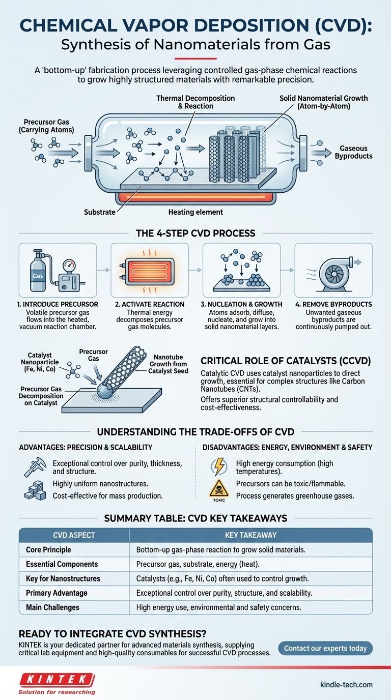
At its core, Chemical Vapor Deposition (CVD) is a synthesis method used to create high-purity solid materials, including nanomaterials, directly from a gas. In this process, a volatile chemical precursor is introduced into a reaction chamber where it decomposes or reacts under heat, causing a new material to deposit and grow on a substrate surface atom by atom. This controlled growth allows for the fabrication of highly ordered nanostructures like thin films and carbon nanotubes.
While often perceived as a coating technique, CVD for nanomaterials is fundamentally a "bottom-up" fabrication process. It leverages controlled gas-phase chemical reactions to grow highly structured materials with remarkable precision directly onto a target substrate.
The CVD Process: From Gas to Solid Nanostructure
CVD is not a single action but a sequence of carefully controlled physical and chemical events. Understanding each step reveals how a simple gas can be transformed into a complex nanomaterial.
The Core Components: Precursor, Substrate, and Energy
The entire process relies on three key elements. The precursor is a volatile gaseous compound containing the atoms needed for the final material. The substrate is the surface or workpiece onto which the nanomaterial will grow. Finally, energy, typically in the form of high heat, is supplied to drive the necessary chemical reactions.
Step 1: Introducing the Precursor Gas
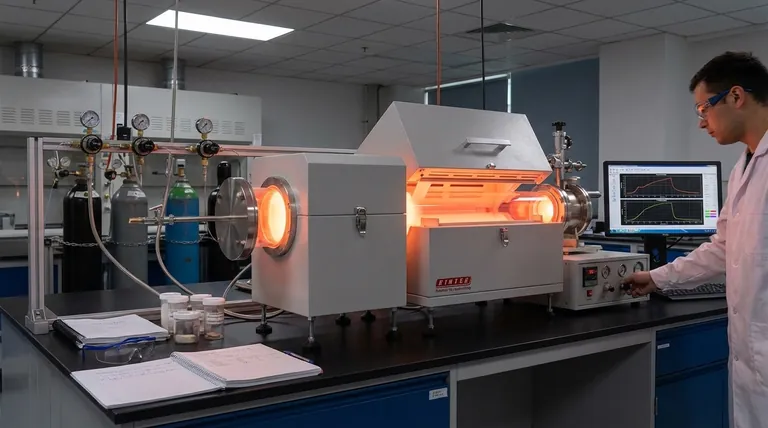
The process begins by placing the substrate into a sealed reaction chamber, which is often held under a vacuum. A carrier gas then transports the volatile precursor gas into this chamber, ensuring it flows over the substrate.
Step 2: Activating the Chemical Reaction
The chamber and substrate are heated to a specific reaction temperature. This thermal energy causes the precursor gas molecules to become unstable and either decompose (break down) or react with other gases present in the chamber.
Step 3: Nucleation and Growth on the Substrate
The decomposed atoms or molecules adsorb onto the hot substrate surface. They then diffuse across the surface to find stable "nucleation sites," where they begin to bond and form the initial seeds of the solid material. Over time, more atoms deposit onto these sites, growing the nanostructure layer by layer into a film, wire, or tube.
Step 4: Removing the Byproducts
The chemical reactions produce the desired solid material as well as unwanted gaseous byproducts. These waste gases are desorbed from the surface and continuously pumped out of the chamber, leaving behind a pure, solid nanostructure on the substrate.
The Critical Role of Catalysts in Nanomaterial Synthesis
For creating specific, complex nanostructures like carbon nanotubes (CNTs), standard CVD is often insufficient. This is where a catalyst becomes essential.
Why Catalysts are Essential
A catalyst provides a specific, energetically favorable site for the chemical reaction to occur. In nanomaterial synthesis, tiny nanoparticles of a catalyst (such as iron, nickel, or cobalt) act as seeds that direct the growth of the material with a specific structure.
How Catalytic CVD (CCVD) Works
In Catalytic CVD (CCVD), the substrate is first coated with a layer of catalyst nanoparticles. When the precursor gas (e.g., a hydrocarbon for making CNTs) is introduced and heated, it selectively decomposes only on the surface of these catalyst particles. The carbon atoms then assemble and extrude outwards from the catalyst, forming a highly structured tube. This method is the mainstream approach for CNTs because it offers superior structural controllability and is highly cost-effective.
Understanding the Trade-offs of CVD
Like any advanced manufacturing process, CVD presents a balance of powerful advantages and significant challenges that must be considered.
Advantage: Precision and Scalability
The primary benefit of CVD is the exceptional control it offers over the purity, thickness, and structure of the final material. Because it builds materials from the atom up, it can produce highly uniform and ordered nanostructures. The process is also highly scalable and cost-effective for mass production.
Disadvantage: High Energy Consumption
CVD is an energy-intensive process. The high temperatures required to trigger the chemical reactions consume a significant amount of power, contributing to operational costs and the overall energy footprint of the fabrication process.
Disadvantage: Environmental and Safety Concerns
The chemical precursors used in CVD can be toxic, flammable, or corrosive, requiring strict safety protocols. Furthermore, the synthesis process itself can generate greenhouse gases and other byproducts that contribute to ecotoxicity, demanding careful management of waste streams to limit environmental impact.
Making the Right Choice for Your Goal
CVD is a powerful and versatile tool, but its suitability depends entirely on your specific objective.
- If your primary focus is high-purity, structurally-defined nanomaterials (like CNTs): Catalytic CVD is the industry-standard method due to its exceptional control over growth and scalability.
- If your primary focus is creating uniform thin films at the nanoscale: CVD is an ideal choice, as it provides an even, conformal layer that can coat complex surfaces with high precision.
- If your primary focus is minimizing environmental impact: You must critically evaluate the specific precursors and operating temperatures required, as these are the main drivers of CVD's ecological footprint and overall cost.
Ultimately, mastering CVD is about precisely controlling a chemical reaction in the gas phase to build functional materials from the atom up.
Summary Table:
| CVD Aspect | Key Takeaway |
|---|---|
| Core Principle | A "bottom-up" process using gas-phase reactions to grow solid materials on a substrate. |
| Essential Components | Precursor gas, substrate, and energy (heat). |
| Key for Nanostructures | Catalysts (e.g., Fe, Ni, Co nanoparticles) are often used to control the growth of materials like carbon nanotubes. |
| Primary Advantage | Exceptional control over material purity, thickness, and structure; highly scalable. |
| Main Challenges | High energy consumption and potential environmental/safety concerns with precursors and byproducts. |
Ready to Integrate CVD Synthesis into Your Laboratory Workflow?
Navigating the complexities of Chemical Vapor Deposition requires not just expertise but also the right, high-purity equipment and consumables. Whether you are developing next-generation carbon nanotubes or depositing uniform thin films, the quality of your precursors, substrates, and reactor components is paramount to achieving precise, reproducible results.
KINTEK is your dedicated partner in advanced materials synthesis. We specialize in supplying the critical lab equipment and high-quality consumables that researchers and engineers rely on for successful CVD processes. From robust reaction chambers to precision catalysts and substrates, we provide the foundational tools for innovation.
Let us help you optimize your CVD operations for superior performance and efficiency.
Contact our experts today to discuss your specific nanomaterial synthesis challenges and discover how our solutions can accelerate your research and development.
Visual Guide
Related Products
- Chemical Vapor Deposition CVD Equipment System Chamber Slide PECVD Tube Furnace with Liquid Gasifier PECVD Machine
- RF PECVD System Radio Frequency Plasma-Enhanced Chemical Vapor Deposition RF PECVD
- Microwave Plasma Chemical Vapor Deposition MPCVD Machine System Reactor for Lab and Diamond Growth
- Customer Made Versatile CVD Tube Furnace Chemical Vapor Deposition Chamber System Equipment
- 915MHz MPCVD Diamond Machine Microwave Plasma Chemical Vapor Deposition System Reactor
People Also Ask
- Why is Chemical Vapor Deposition (CVD) equipment uniquely suited for constructing hierarchical superhydrophobic structures?
- What is the chemical vapor deposition growth process? Build Superior Thin Films from the Atom Up
- How are carbon nanotubes grown? Master Scalable Production with Chemical Vapor Deposition
- How expensive is chemical vapor deposition? Understanding the True Cost of High-Performance Coating
- What are the advantages of chemical vapor deposition? Achieve Superior Thin Films for Your Lab


