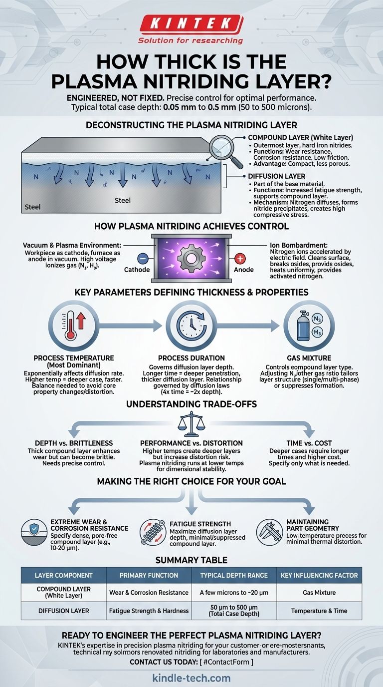
To be precise, there is no single thickness for a plasma nitriding layer. The layer's depth is an engineered outcome, not a fixed property. It is precisely controlled based on the material and desired performance, but a typical total case depth can range from 0.05 mm to 0.5 mm (50 to 500 microns).
The thickness of a nitrided layer is less important than its structure. The true value of plasma nitriding lies in its ability to precisely control the formation of two distinct layers—a hard outer compound layer and a deep, strong diffusion layer—to achieve specific engineering goals like wear or fatigue resistance.
Deconstructing the Plasma Nitriding Layer
To understand the thickness, you must first understand the two distinct zones that comprise the full layer. Each serves a different function and their relative depths are engineered for the application.
The Compound Layer (White Layer)
This is the outermost layer, often called the "white layer." It is composed of hard iron nitride phases (such as ε and γ’).
This layer is directly responsible for wear resistance, corrosion resistance, and providing a low-friction surface. A key advantage of plasma nitriding is that it produces a more compact and less porous compound layer than older methods like gas nitriding.
The Diffusion Layer
Beneath the compound layer lies the diffusion layer. This zone is not a coating but is part of the original base material.
Here, nitrogen atoms have diffused into the steel's crystal lattice, forming fine nitride precipitates with alloying elements. This creates high compressive stress and increases hardness, which is critical for improving fatigue strength and supporting the hard compound layer.
How Plasma Nitriding Achieves Control
The plasma nitriding process itself is what allows for such precise control over the final surface properties. It is a vacuum-supported thermochemical process.
The Vacuum and Plasma Environment
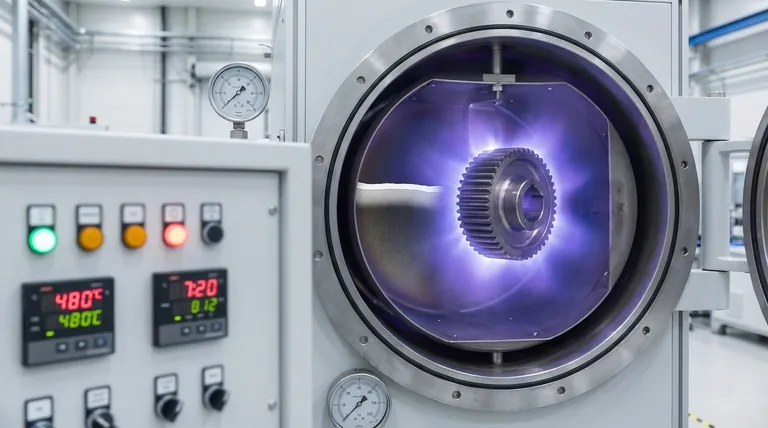
Workpieces are placed in a vacuum chamber and form the cathode (negative terminal). The furnace wall acts as the anode. When a high voltage is applied, the treatment gas (primarily nitrogen and hydrogen) ionizes, forming a glowing plasma around the parts.
The Role of Ion Bombardment
Nitrogen ions from the plasma are accelerated by the electric field and strike the workpiece surface with high energy.
This ion bombardment has several effects: it cleans the surface at a microscopic level, breaks down any passive oxide layers, heats the workpiece uniformly, and provides the activated nitrogen that diffuses into the material to form the nitriding layer.
Key Parameters That Define Layer Thickness and Properties
The final structure and thickness of the nitrided case are a direct result of controlling three key process parameters.
Process Temperature
Temperature is the most dominant factor. The rate of nitrogen diffusion into the steel is exponentially affected by temperature.
Higher temperatures increase the diffusion rate, leading to a deeper case in less time. However, this must be carefully balanced to avoid unwanted changes to the core properties of the material or part distortion.
Process Duration
The duration of the treatment directly influences the depth of the diffusion layer. The relationship is governed by diffusion laws, meaning achieving double the depth requires roughly four times the process duration.
Longer cycle times allow nitrogen to penetrate deeper into the material, thickening the diffusion layer and increasing fatigue resistance.
Gas Mixture
The composition of the process gas is used to control the formation and type of the compound layer. By adjusting the ratio of nitrogen to other gases, operators can tailor the surface to be a single-phase or multi-phase nitride layer, or even suppress its formation entirely if only a diffusion layer is desired.
Understanding the Trade-offs
Specifying a plasma nitriding process involves balancing competing objectives. You cannot maximize all properties simultaneously.
Depth vs. Brittleness
While a thick compound layer enhances wear resistance, it can also become brittle if it grows too thick, potentially flaking off in service. Precise process control is needed to create a compound layer that is hard and dense but not excessively thick.
Performance vs. Distortion
Higher process temperatures (e.g., 500-520°C) create deeper layers faster, but they also increase the risk of thermal distortion, especially in precision parts. Plasma nitriding's ability to run at lower temperatures (as low as 350°C) is a major advantage for maintaining dimensional stability.
Time vs. Cost
Deeper case depths require significantly longer process times. Since furnace time is a primary cost driver, specifying an unnecessarily deep case is inefficient and expensive. The depth should be no more than is required for the application.
Making the Right Choice for Your Goal
The ideal plasma nitriding specification depends entirely on the component's primary function.
- If your primary focus is extreme wear and corrosion resistance: Specify a process that develops a dense, pore-free compound layer of a specific thickness (e.g., 10-20 microns).
- If your primary focus is fatigue strength: Specify a process that maximizes the depth of the diffusion layer, often with a minimal or suppressed compound layer.
- If your primary focus is maintaining part geometry: Specify a low-temperature process that minimizes thermal distortion while still achieving the necessary surface hardness.
Ultimately, effective surface engineering is about defining the problem first, then specifying the precise layer structure needed to solve it.
Summary Table:
| Layer Component | Primary Function | Typical Depth Range | Key Influencing Factor |
|---|---|---|---|
| Compound Layer (White Layer) | Wear & Corrosion Resistance | A few microns to ~20 µm | Gas Mixture |
| Diffusion Layer | Fatigue Strength & Hardness | 50 µm to 500 µm (Total Case Depth) | Temperature & Time |
Ready to engineer the perfect plasma nitriding layer for your components?
Specifying the right case depth and structure is critical for performance and cost-efficiency. The experts at KINTEK specialize in precision plasma nitriding services for laboratories and manufacturers. We help you balance wear resistance, fatigue strength, and dimensional stability to meet your exact engineering goals.
Contact us today using the form below to discuss your application and receive a tailored solution. Let KINTEK's expertise in lab equipment and surface engineering enhance your product's performance and longevity.
Visual Guide
Related Products
People Also Ask
- What are pure silicon sputtering targets? Precision Source for High-Performance Thin Films
- What types of ceramics are used in sintering? Expert Guide to Advanced Materials and Forming
- Which is the most preferred material for manufacturing of a semiconductor? Silicon's Dominance Explained
- What are the methods of high temperature ceramic? Master the 3-Stage Process for Durable Components
- Can silicon be sputtered? A Guide to RF & DC Methods for Thin Film Deposition
