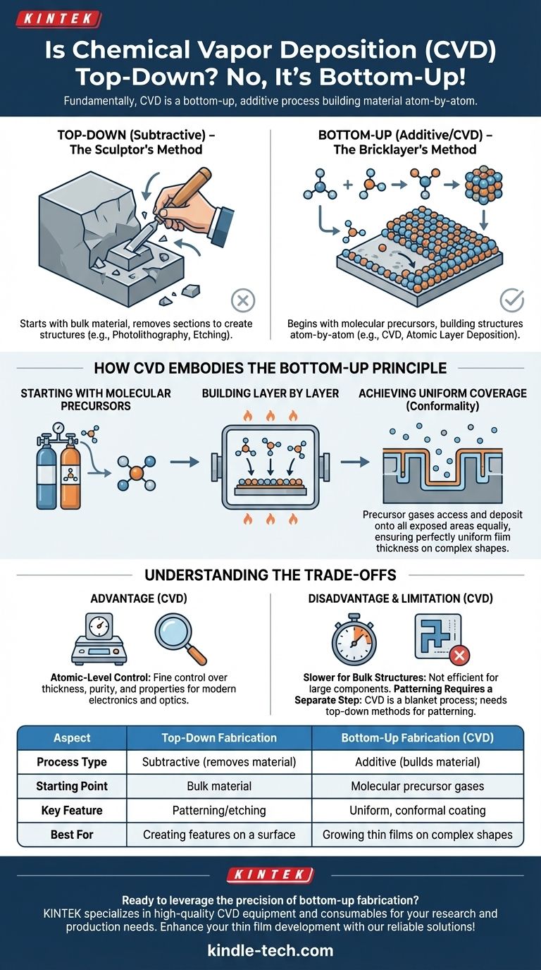
Fundamentally, Chemical Vapor Deposition (CVD) is not a top-down process; it is a quintessential example of bottom-up fabrication. Top-down methods involve starting with a larger piece of material and removing sections, much like a sculptor carves stone. In contrast, CVD is an additive process that builds a new layer of material atom-by-atom or molecule-by-molecule onto a surface.
The distinction is more than academic. Recognizing CVD as a "bottom-up" technique is critical to understanding its core strength: the ability to grow highly uniform, pure, and precisely controlled thin films, even over complex three-dimensional surfaces.
What Defines "Top-Down" vs. "Bottom-Up" Fabrication?
To understand where CVD fits, we must first clearly define the two major paradigms in manufacturing and material fabrication.
The "Top-Down" Approach: The Sculptor's Method
Top-down fabrication starts with a bulk material, or substrate. Material is then selectively removed to create the desired pattern or structure.
Think of photolithography in semiconductor manufacturing. You start with a full silicon wafer and use light and chemicals to etch away unwanted portions, leaving behind the intricate circuits. This is a subtractive process.
The "Bottom-Up" Approach: The Bricklayer's Method
Bottom-up fabrication is the reverse. It begins with atomic or molecular precursors and assembles them into a larger, more complex structure.
This is an additive process. Instead of carving from a block, you are meticulously laying individual bricks to build a wall. CVD operates precisely on this principle.
How Chemical Vapor Deposition Embodies the Bottom-Up Principle
The mechanics of the CVD process align perfectly with the bottom-up, or additive, manufacturing model.
Starting with Molecular Precursors
The CVD process does not begin with a solid block to be carved. It starts with a volatile precursor gas—the molecular "bricks" for the new layer.
These gases are introduced into a vacuum chamber containing the object to be coated, known as the substrate.
Building Layer by Layer
When the chamber is heated, the precursor gas molecules react or decompose near the substrate's surface.
The resulting atoms or molecules bond to the surface, gradually building up the desired coating over time. The film grows upwards from the substrate, one layer of atoms at a time.
Achieving Uniform Coverage (Conformality)
A key advantage of this bottom-up method is its ability to create a conformal coating.
Because the process relies on a gas, the precursor molecules can access and deposit onto all exposed areas of the substrate equally, ensuring a perfectly uniform film thickness even inside crevices or over complex shapes.
Understanding the Trade-offs
While powerful, the bottom-up nature of CVD comes with its own set of considerations compared to top-down methods.
Advantage: Atomic-Level Control
CVD offers exceptionally fine control over the thickness, purity, and properties of the deposited film. This precision is essential for modern electronics, optics, and protective coatings.
Disadvantage: Slower Build Rates for Bulk Structures
CVD is designed for creating thin films, typically measured in nanometers or micrometers. It is not an efficient method for creating large, bulk structural components, where a top-down machining approach would be far faster.
Limitation: Patterning Requires a Separate Step
CVD itself is a blanket deposition process; it coats everything exposed to the gas. To create specific patterns, CVD must be combined with a top-down process like lithography and etching to selectively remove the deposited film.
Making the Right Choice for Your Goal
Understanding this distinction allows you to select the right approach for your specific engineering challenge.
- If your primary focus is creating a thin, uniform, high-purity coating: CVD's bottom-up nature is the ideal choice, especially for coating complex geometries.
- If your primary focus is patterning or creating features on a bulk material: A top-down approach like photolithography and etching is the necessary tool for selectively removing material.
- If your primary focus is creating a large, three-dimensional object: Neither method is ideal; a different additive process like 3D printing or a subtractive method like CNC machining would be more appropriate.
Ultimately, classifying processes as "bottom-up" or "top-down" provides a powerful framework for understanding their fundamental capabilities and limitations.
Summary Table:
| Aspect | Top-Down Fabrication | Bottom-Up Fabrication (CVD) |
|---|---|---|
| Process Type | Subtractive (removes material) | Additive (builds material) |
| Starting Point | Bulk material | Molecular precursor gases |
| Key Feature | Patterning/etching | Uniform, conformal coating |
| Best For | Creating features on a surface | Growing thin films on complex shapes |
Ready to leverage the precision of bottom-up fabrication in your lab? KINTEK specializes in providing high-quality CVD equipment and consumables tailored to your laboratory's needs. Whether you're developing advanced thin films for semiconductors, optics, or protective coatings, our solutions ensure superior performance and reliability. Contact us today to discuss how our expertise can enhance your research and production processes!
Visual Guide
Related Products
- Chemical Vapor Deposition CVD Equipment System Chamber Slide PECVD Tube Furnace with Liquid Gasifier PECVD Machine
- RF PECVD System Radio Frequency Plasma-Enhanced Chemical Vapor Deposition RF PECVD
- Microwave Plasma Chemical Vapor Deposition MPCVD Machine System Reactor for Lab and Diamond Growth
- Customer Made Versatile CVD Tube Furnace Chemical Vapor Deposition Chamber System Equipment
- 915MHz MPCVD Diamond Machine Microwave Plasma Chemical Vapor Deposition System Reactor
People Also Ask
- What is the chemical vapor deposition growth process? Build Superior Thin Films from the Atom Up
- What happens during deposition chemistry? Building Thin Films from Gaseous Precursors
- What are the advantages of chemical vapor deposition? Achieve Superior Thin Films for Your Lab
- What are the processes of vapor phase deposition? Understand CVD vs. PVD for Superior Thin Films
- What types of substrates are used in CVD to facilitate graphene films? Optimize Graphene Growth with the Right Catalyst


