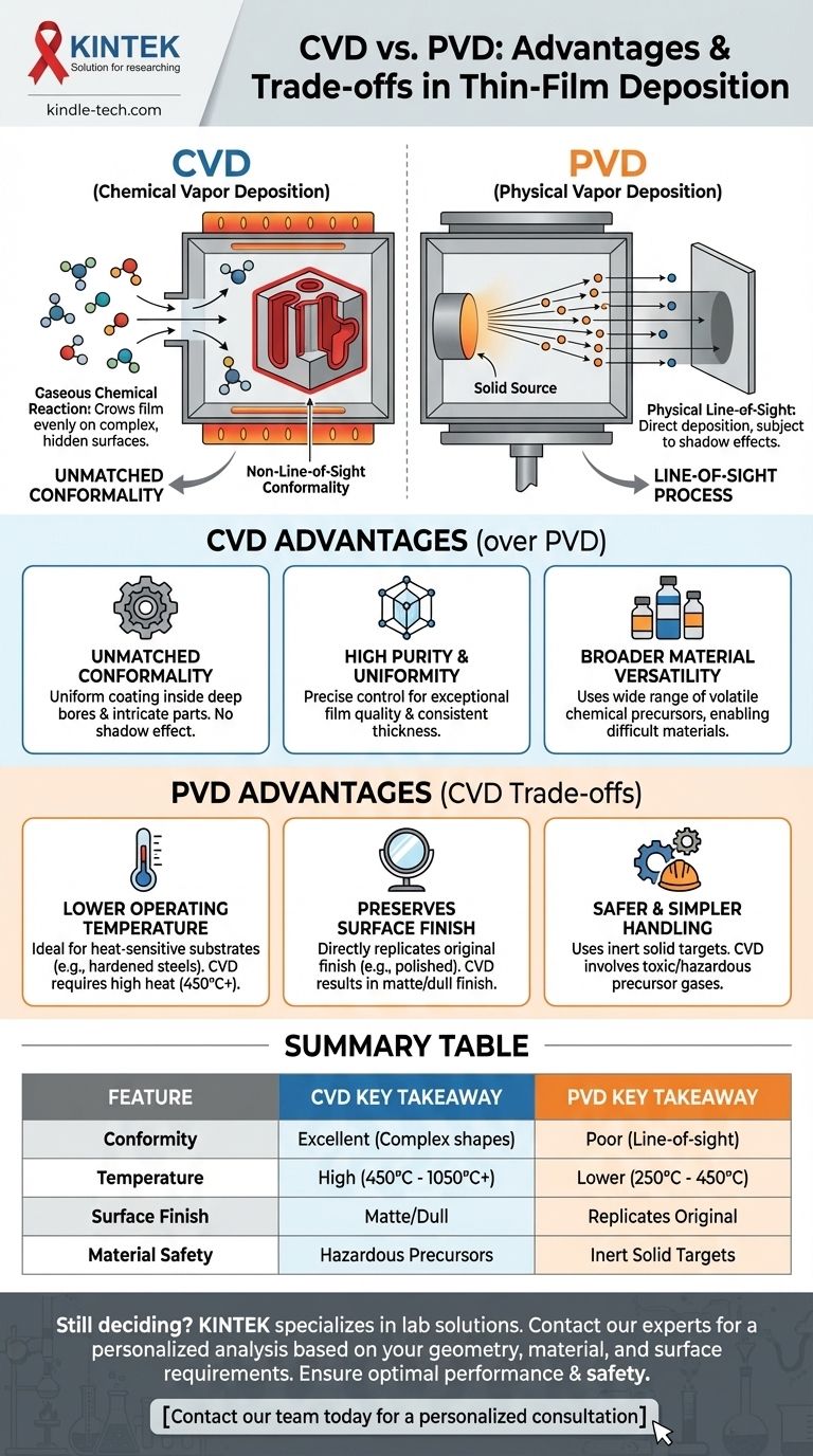
When choosing a thin-film deposition method, the primary advantages of Chemical Vapor Deposition (CVD) over Physical Vapor Deposition (PVD) are its ability to create highly uniform coatings on complex, non-line-of-sight surfaces and its versatility in using a wider range of materials. Because CVD is a chemical process rather than a physical one, it can "grow" a film evenly inside deep holes or on intricate shapes where PVD would be blocked.
CVD's core strength is its chemical reaction-based process, enabling superior coating conformity on complex geometries. However, this advantage is balanced by significant trade-offs, primarily high operating temperatures and the handling of hazardous materials, which makes PVD a more suitable choice for many applications.
The Fundamental Difference: Chemical Reaction vs. Physical Deposition
To understand the advantages of each method, you must first grasp how they fundamentally differ. The choice between CVD and PVD is a choice between a chemical growth process and a physical coating process.
How CVD Works: A Gaseous Chemical Reaction
In CVD, one or more volatile precursor gases are introduced into a reaction chamber. These gases decompose and react on the heated surface of the substrate, forming a solid film.
This process is more like growing a crystal layer across the entire exposed surface, as the gas molecules can reach every nook and cranny before reacting.
How PVD Works: A Line-of-Sight Process
In PVD, a solid source material is vaporized in a vacuum through methods like sputtering or evaporation. These vaporized atoms travel in a straight line and physically impinge upon the substrate, condensing to form a film.
This is analogous to spray painting; any area not in the direct line of sight of the spray nozzle will receive little to no coating, creating a "shadow effect."
Key Advantages of CVD Explained
The chemical nature of CVD gives it distinct advantages in specific scenarios where PVD would fall short.
Unmatched Conformality: Coating Beyond the Line of Sight
Because CVD relies on gases that fill the entire chamber, it is not limited by line-of-sight effects. It can deposit a uniform, conformal coating inside deep bores, channels, and on highly complex 3D parts.
This is the single most important advantage and the primary reason to choose CVD for components with intricate internal geometries.
High Purity and Uniformity
The chemical reactions in CVD can be controlled with high precision. This allows for the creation of exceptionally high-purity films with a very uniform grain structure and thickness across the entire part.
Broader Material Versatility
CVD can be used with any element or compound that can be delivered as a volatile chemical precursor. This opens up possibilities for materials that are extremely difficult or inefficient to evaporate from a solid target, as required by PVD.
Understanding the Trade-offs: The Case for PVD
CVD's advantages come with significant operational challenges. For many applications, these trade-offs make PVD the more practical and effective choice.
The Critical Role of Temperature
CVD typically operates at very high temperatures (450°C to over 1050°C) to drive the necessary chemical reactions. PVD operates at much lower temperatures (250°C to 450°C).
This high heat means CVD can damage or alter the properties of many substrate materials, such as hardened steels or aluminum alloys. PVD is the default choice for coating finished, heat-sensitive components.
Surface Finish and Aesthetics
PVD directly replicates the substrate's original surface finish. If you coat a polished part with PVD, it will remain polished.
CVD, due to its crystal growth process, typically results in a matte or dull finish. Achieving a polished look on a CVD-coated part requires costly and time-consuming post-processing.
Safety and Handling Concerns
The precursor gases used in many CVD processes can be toxic, pyrophoric, or corrosive. This necessitates complex and expensive safety protocols, storage, and handling infrastructure.
PVD uses solid, inert target materials, making it a fundamentally safer and simpler process from a material handling perspective.
Making the Right Choice for Your Goal
Your decision must be driven by the non-negotiable requirements of your component and material.
- If your primary focus is coating complex internal geometries or achieving the highest possible purity: CVD is the superior choice due to its non-line-of-sight, chemical reaction-based deposition.
- If your primary focus is coating heat-sensitive materials or preserving a specific surface finish: PVD is the more practical and safer option due to its lower operating temperatures and direct deposition nature.
- If your primary focus is operational simplicity and safety for common applications: PVD presents a lower barrier to entry regarding equipment, material handling, and post-processing requirements.
By understanding this core trade-off between CVD's conformity and PVD's lower-temperature versatility, you can confidently select the technology that aligns with your material's limits and your product's ultimate function.
Summary Table:
| Advantage of CVD | Key Takeaway |
|---|---|
| Conformity | Uniformly coats complex, non-line-of-sight surfaces (e.g., deep holes). |
| Material Versatility | Uses a wider range of materials via gaseous precursors. |
| Film Purity & Uniformity | Enables high-purity, uniform grain structure and thickness. |
| Trade-off: Temperature | Requires high heat (450°C+), which can damage heat-sensitive substrates. |
| Trade-off: Surface Finish | Typically results in a matte finish, unlike PVD's direct replication. |
Still deciding between CVD and PVD for your specific application?
KINTEK specializes in lab equipment and consumables, serving laboratory needs. Our experts can help you analyze your project's requirements—whether you need the unmatched conformity of CVD for complex geometries or the lower-temperature versatility of PVD for heat-sensitive materials. We provide the right solutions to enhance your thin-film deposition process, ensuring optimal performance, safety, and efficiency.
Contact our team today for a personalized consultation and let KINTEK help you make the right choice for your laboratory's success.
Visual Guide
Related Products
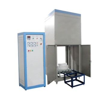
- Inclined Rotary Plasma Enhanced Chemical Vapor Deposition PECVD Equipment Tube Furnace Machine
- HFCVD Machine System Equipment for Drawing Die Nano-Diamond Coating
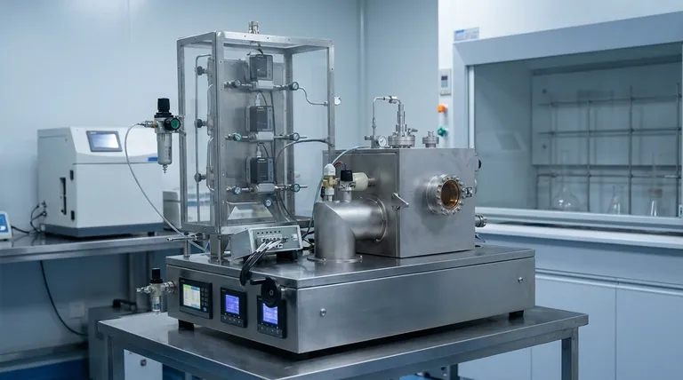
- 915MHz MPCVD Diamond Machine Microwave Plasma Chemical Vapor Deposition System Reactor
- Vacuum Hot Press Furnace Machine for Lamination and Heating
- 1200℃ Split Tube Furnace with Quartz Tube Laboratory Tubular Furnace
People Also Ask
- What materials are deposited in PECVD? Discover the Versatile Thin-Film Materials for Your Application
- What is plasma enhanced chemical vapour deposition process? Unlock Low-Temperature, High-Quality Thin Films
- What is plasma enhanced chemical vapor deposition? Achieve Low-Temperature, High-Quality Thin Films
- What is PECVD used for? Achieve Low-Temperature, High-Performance Thin Films
- What is PECVD silicon deposition? Achieve Low-Temperature, High-Quality Thin Films