From a materials science perspective, diamond semiconductors offer a revolutionary leap in performance for electronics operating under extreme conditions. Their primary advantages over silicon include the ability to handle significantly higher power, operate at much higher frequencies, and withstand extreme temperatures, all driven by a unique combination of fundamental physical properties.
While silicon has defined modern electronics, diamond represents a theoretical next frontier for devices pushed to their absolute limits. Its core advantages promise not just incremental improvements but order-of-magnitude gains in power handling and heat management, though immense manufacturing challenges currently prevent widespread use.
The Fundamental Properties Driving Diamond's Potential
The theoretical benefits of diamond are not arbitrary; they are direct consequences of its unique atomic structure and the strong covalent bonds between its carbon atoms. These properties give it a clear edge in several key areas.
Unmatched Thermal Conductivity
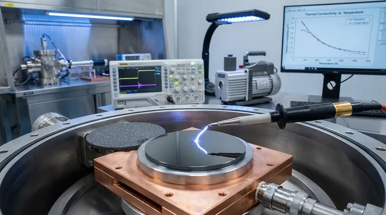
Diamond is the most thermally conductive material known at room temperature, exceeding copper by a factor of five and silicon by more than an order of magnitude.
This means it can dissipate waste heat with unparalleled efficiency. For a semiconductor, this is like having a perfect, built-in heat sink, allowing for much denser and more powerful circuits without the risk of thermal failure.
Ultra-Wide Bandgap
A semiconductor's bandgap is the energy required to excite an electron into a conductive state. Diamond has an ultra-wide bandgap of approximately 5.5 electron volts (eV), compared to silicon's 1.1 eV.
This wide bandgap directly enables two critical capabilities. First, it allows devices to operate at much higher temperatures before electrons start leaking across the gap, maintaining stability. Second, it allows the material to withstand much higher internal electric fields before breaking down.
Extreme Electric Breakdown Field
The breakdown field is the maximum voltage a material can endure before it fails catastrophically. Diamond's breakdown field is over 20 times greater than that of silicon.
This allows for the creation of power devices that are dramatically smaller, lighter, and more efficient for the same voltage rating. It is the key enabler for next-generation high-voltage power electronics.
High Carrier Mobility
Carrier mobility measures how quickly charge carriers (electrons and holes) can move through a material when a voltage is applied. While not the absolute highest, diamond possesses very high mobility for both electrons and holes.
This property is crucial for high-frequency applications. Faster-moving carriers allow transistors to switch on and off more rapidly, enabling devices that can operate in the high gigahertz or even terahertz range, essential for future communication systems like 6G.
Understanding the Trade-offs: The Challenge of Reality
If diamond is so superior, its absence from the market requires explanation. The theoretical advantages are countered by profound and practical challenges that have relegated it to laboratory and niche applications.
The Doping Problem
As noted, pure diamond is a natural insulator. To function as a semiconductor, it must be "doped" with impurities to introduce charge carriers. Due to its incredibly dense and stable crystal lattice, this is extremely difficult.
Achieving effective and controllable n-type doping (adding electrons) has been a particularly stubborn, long-standing problem for materials scientists, hindering the creation of basic components like diodes and transistors.
Manufacturing and Cost
Silicon manufacturing is a mature, scaled, and relatively inexpensive process that produces massive, near-perfect single-crystal wafers.
In contrast, growing large, high-quality, single-crystal diamond wafers is an exceptionally slow and expensive process. This economic barrier is perhaps the single greatest obstacle to commercial viability for most applications.
High Contact Resistance
Simply making a good electrical connection to diamond is a non-trivial engineering challenge. The difficulty in forming low-resistance ohmic contacts can introduce parasitic effects that negate some of the material's intrinsic performance benefits.
How to Apply This to Your Project
Evaluating diamond's role depends entirely on the performance demands of your application. It is not a replacement for silicon but a solution for problems silicon cannot solve.
- If your primary focus is high-power electronics or grid applications: Diamond's high voltage and thermal capabilities promise smaller, more efficient power converters and inverters.
- If your primary focus is high-frequency communications (e.g., 6G and beyond): Its high carrier mobility makes it a leading candidate for next-generation radio frequency transistors and amplifiers.
- If your primary focus is devices for extreme environments (space, defense, industrial sensing): Diamond's ability to operate at extreme temperatures and in high-radiation environments without external cooling is its most compelling advantage.
Ultimately, diamond semiconductors represent a frontier technology where immense theoretical advantages are locked in a battle with fundamental manufacturing and engineering challenges.
Summary Table:
| Key Advantage | Benefit for Electronics |
|---|---|
| Unmatched Thermal Conductivity | Superior heat dissipation, enabling denser, more powerful circuits. |
| Ultra-Wide Bandgap (5.5 eV) | Stable operation at extreme temperatures and high internal electric fields. |
| Extreme Electric Breakdown Field | Smaller, lighter, and more efficient high-voltage power devices. |
| High Carrier Mobility | Enables high-frequency operation for next-gen communications (e.g., 6G). |
Ready to push the limits of your electronics?
Diamond semiconductors offer a revolutionary leap in performance for high-power, high-frequency, and extreme-temperature applications. If your project involves power electronics, next-generation communications (6G), or devices for harsh environments (space, defense, industrial sensing), the unique properties of diamond could be your key to success.
At KINTEK, we specialize in providing advanced lab equipment and consumables to support cutting-edge materials science research and development. Our expertise can help you explore the potential of diamond semiconductors for your specific needs.
Contact our experts today to discuss how we can support your laboratory's journey into next-generation semiconductor technology.
Visual Guide

Related Products
- CVD Diamond Domes for Industrial and Scientific Applications
- Laboratory CVD Boron Doped Diamond Materials
- CVD Diamond Wire Drawing Die Blanks for Precision Applications
- 915MHz MPCVD Diamond Machine Microwave Plasma Chemical Vapor Deposition System Reactor
- CVD Diamond for Thermal Management Applications
People Also Ask
- What color diamonds are CVD? Understanding the Process from Brown Tint to Colorless Beauty
- Are CVD diamonds worth it? Unlock Brilliant Value & Ethical Clarity
- How do CVD diamonds grow? A Step-by-Step Guide to Lab-Grown Diamond Creation
- What is chemical vapor deposition of diamond? Grow High-Purity Diamonds Atom-by-Atom
- Do all CVD diamonds have post growth treatment? Uncovering the Industry Standard for Gem Quality