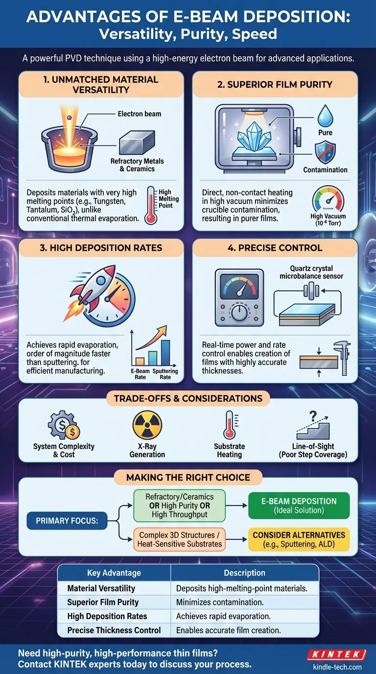
In essence, electron beam deposition offers a powerful combination of material versatility, high purity, and speed. This physical vapor deposition (PVD) technique uses a high-energy electron beam to evaporate source materials, making it uniquely capable of depositing materials with very high melting points, such as refractory metals and ceramics. This process occurs in a high vacuum, which, combined with direct heating of the source material, results in exceptionally pure thin films at high deposition rates.
While many deposition methods exist, e-beam evaporation stands out for its unique ability to handle the most challenging materials. It is the go-to technique when you need to create high-purity films from refractory metals or dielectrics, and when production speed is a critical factor.
Why Choose E-Beam Deposition?
Understanding the core mechanics of e-beam deposition reveals why it is a preferred method for advanced applications in optics, electronics, and materials science. The process's advantages stem directly from its use of a focused, high-energy electron beam as the heating source.
Unmatched Material Versatility
E-beam deposition excels where other thermal processes fail. The intense, localized energy from the electron beam can melt and evaporate virtually any material.
This makes it the ideal choice for depositing refractory metals like tungsten, tantalum, and molybdenum, which have melting points far too high for conventional thermal evaporation boats. It is also highly effective for dielectric compounds such as silicon dioxide (SiO₂) and titanium dioxide (TiO₂), which are fundamental to optical coatings.
Superior Film Purity
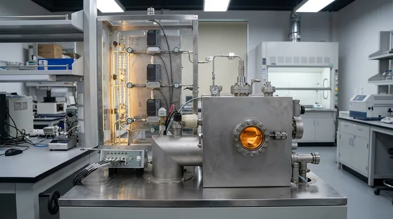
Purity is often a non-negotiable requirement, and e-beam delivers. The electron beam directly heats the source material (the "puck") in a water-cooled copper hearth.
Because the heating element (the electron beam) is not in physical contact with the material, contamination from a crucible or boat is virtually eliminated. This, combined with the high-vacuum environment (typically 10⁻⁶ Torr or lower), minimizes the incorporation of residual gas atoms into the growing film, resulting in a significantly purer final product compared to thermal evaporation.
High Deposition Rates and Efficiency
For manufacturing and rapid prototyping, speed matters. E-beam can achieve deposition rates that are an order of magnitude higher than techniques like sputtering.
This high rate is a direct result of the high power density that can be focused onto the source material, leading to rapid evaporation. Furthermore, since the beam heats only a small portion of the source, material usage is highly efficient, which is a critical cost-saving factor when working with precious materials like gold or platinum.
Precise Control Over Film Structure
The system allows for fine-tuning of the final film properties. The deposition rate is directly proportional to the electron beam's power, which can be precisely controlled in real-time.
This control, often coupled with a quartz crystal microbalance (QCM) for feedback, allows for the creation of films with highly accurate thicknesses. The line-of-sight nature of the deposition also enables the use of shadow masks to create specific patterns on the substrate.
Understanding the Trade-offs and Limitations
No technique is perfect. Being a trusted advisor means acknowledging the limitations of e-beam deposition so you can make an informed decision.
System Complexity and Cost
E-beam systems are more complex and expensive than their thermal evaporation counterparts. They require high-voltage power supplies, magnetic fields for beam steering, and robust cooling systems, all of which increase the initial investment and maintenance overhead.
X-Ray Generation
A critical safety and operational concern is the generation of X-rays. When high-energy electrons strike the target material, they produce bremsstrahlung radiation. This requires appropriate lead shielding to protect operators and can potentially damage sensitive electronic substrates or components if they are not properly protected.
Substrate Heating
The intense energy required for evaporation also produces significant radiant heat. This can cause an undesirable temperature increase on the substrate, potentially damaging heat-sensitive materials like polymers or certain semiconductor devices.
Line-of-Sight Deposition Issues
E-beam is a "point source," line-of-sight technique. This means it can struggle to coat the sidewalls of features on a substrate, a phenomenon known as poor step coverage. Achieving uniform coating thickness across large-area substrates also requires complex planetary substrate holders that rotate the samples during deposition.
Making the Right Choice for Your Goal
Selecting a deposition technique depends entirely on your project's specific constraints and desired outcomes.
- If your primary focus is depositing refractory metals or ceramics: E-beam deposition is the superior, and often the only, viable choice.
- If your primary focus is achieving the highest possible film purity: E-beam is a leading option, significantly outperforming standard thermal evaporation.
- If your primary focus is high-throughput production: The high deposition rates of e-beam make it an extremely attractive option for manufacturing environments.
- If your primary focus is coating complex 3D structures or using heat-sensitive substrates: You should carefully evaluate alternatives like sputtering or atomic layer deposition (ALD), which offer better conformality and lower thermal load.
By understanding its distinct advantages and inherent trade-offs, you can confidently determine if e-beam deposition is the right tool to achieve your technical goals.
Summary Table:
| Key Advantage | Description |
|---|---|
| Material Versatility | Deposits high-melting-point materials like tungsten, tantalum, and ceramics. |
| Superior Film Purity | Minimizes contamination with direct, non-contact heating in a high vacuum. |
| High Deposition Rates | Achieves rapid evaporation for efficient manufacturing and prototyping. |
| Precise Thickness Control | Enables accurate film creation with real-time power and rate control. |
Need to deposit high-purity, high-performance thin films?
E-beam deposition is the ideal solution for demanding applications in optics, electronics, and materials science, especially when working with refractory metals or requiring high throughput. KINTEK specializes in advanced lab equipment, including PVD systems, to meet your specific research and production needs.
Contact our experts today to discuss how our solutions can enhance your thin-film processes and achieve your technical goals.
Visual Guide
Related Products
- Electron Beam Evaporation Coating Oxygen-Free Copper Crucible and Evaporation Boat
- Molybdenum Tungsten Tantalum Evaporation Boat for High Temperature Applications
- Electron Beam Evaporation Coating Tungsten Crucible and Molybdenum Crucible for High Temperature Applications
- E Beam Crucibles Electron Gun Beam Crucible for Evaporation
- Electron Beam Evaporation Coating Gold Plating Tungsten Molybdenum Crucible for Evaporation
People Also Ask
- What is the deposition rate of e-beam evaporation? Control Thin Film Quality and Speed
- What is e-beam evaporation used for? Precision Coating for Optics, Aerospace & Electronics
- What is the container that holds the metal source material called in e-beam evaporation? Ensure Purity and Quality in Your Thin-Film Deposition
- What is the temperature of e-beam evaporation? Mastering the Two-Zone Thermal Process for Precision Films
- What are the applications of electron beams? From Nanoscale Imaging to Industrial Manufacturing


