In summary, the primary advantages of e-beam evaporation are its ability to deposit high-purity films from a vast range of materials, including those with very high melting points, at exceptionally high deposition rates. This combination of purity, versatility, and speed makes it a superior choice for demanding applications like precision optical coatings and efficient, large-scale production.
Electron-beam evaporation is not just another deposition method; it is a specialized tool that uniquely balances high throughput with exceptional film purity. Understanding when to leverage its distinct strengths is key to achieving optimal results in thin film engineering.
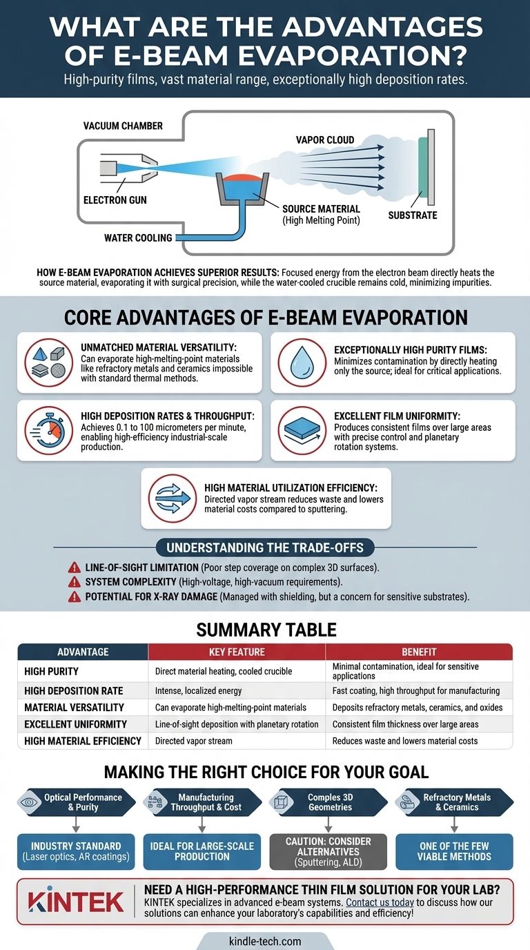
How E-Beam Evaporation Achieves Superior Results
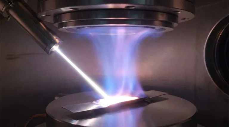
Electron-beam (e-beam) evaporation is a physical vapor deposition (PVD) process. It operates by focusing a high-energy beam of electrons onto a source material held in a cooled crucible.
The Role of Focused Energy
The electron beam directly heats a small spot on the source material, causing it to evaporate or sublimate. This process transfers a massive amount of energy with surgical precision.
Because the crucible itself is water-cooled and remains relatively cold, there is virtually no risk of the crucible material melting or outgassing. This direct heating method is the primary reason for the exceptionally low impurity levels in the final film.
Creating a Vapor Cloud
Once the material vaporizes, it travels in a straight line through the high-vacuum chamber until it condenses on the target substrate. This line-of-sight trajectory gives the process excellent directionality.
Core Advantages of E-Beam Evaporation
The unique mechanism of e-beam evaporation provides several distinct advantages over other deposition techniques like thermal evaporation or sputtering.
Unmatched Material Versatility
Because the electron beam can generate intense, localized heat, it can evaporate materials with extremely high melting points. This includes refractory metals, ceramics, and dielectric oxides that are impossible to deposit using standard thermal evaporation.
Exceptionally High Purity Films
The process minimizes contamination. By only heating the source material and keeping the surrounding crucible cool, the risk of incorporating unwanted impurities into the film is dramatically reduced. This makes e-beam ideal for applications where material purity is critical.
High Deposition Rates and Throughput
E-beam evaporation can achieve very high deposition rates, ranging from 0.1 to 100 micrometers per minute. This speed translates directly to higher manufacturing throughput, making it an efficient choice for industrial-scale production of solar panels or architectural glass.
Excellent Film Uniformity
When paired with a planetary rotation system (which rotates and revolves the substrates) and properly designed masks, e-beam can produce films with excellent thickness uniformity over large areas. The inherent directionality of the vapor stream allows for precise control.
High Material Utilization Efficiency
The process is highly efficient, as the vapor is directed toward the substrate. Compared to a process like sputtering, where material is ejected over a wider angle, e-beam wastes less of the valuable source material, which can significantly reduce costs.
Compatibility with Ion Assist
E-beam systems are often integrated with a secondary ion-assist source (IAD). This allows for pre-cleaning the substrate with an ion beam or bombarding the film during deposition to create denser, more durable coatings with stronger adhesion.
Understanding the Trade-offs
No technology is without its limitations. Being aware of the trade-offs is critical for making an informed decision.
The Line-of-Sight Limitation
The directional nature of e-beam is both a strength and a weakness. It is not well-suited for conformally coating complex, three-dimensional surfaces with deep trenches or undercuts. The vapor travels in a straight line and has difficulty coating "shadowed" areas, a phenomenon known as poor step coverage.
System Complexity
E-beam systems involve high-voltage electron guns and require a high-vacuum environment to operate. This makes them more complex and expensive to purchase, operate, and maintain than simpler methods like thermal evaporation.
Potential for X-Ray Damage
The high-energy electron beam can generate X-rays as a byproduct. While typically managed with shielding, this can be a concern for sensitive substrates or electronic components, which may suffer radiation damage during the coating process.
Making the Right Choice for Your Goal
Selecting the correct deposition method depends entirely on your project's non-negotiable requirements.
- If your primary focus is optical performance and purity: E-beam is the industry standard for creating multi-layer, low-contamination films for laser optics, filters, and AR coatings.
- If your primary focus is manufacturing throughput and cost-efficiency: The high deposition rates and excellent material utilization of e-beam make it ideal for large-scale production.
- If your primary focus is coating complex 3D geometries: You should exercise caution with e-beam and consider alternative methods like sputtering or atomic layer deposition (ALD) for superior step coverage.
- If your primary focus is depositing refractory metals or ceramics: E-beam is one of the few viable methods capable of evaporating materials with very high melting points.
Ultimately, e-beam evaporation offers a powerful solution for creating high-quality thin films when its specific advantages align with your application's needs.
Summary Table:
| Advantage | Key Feature | Benefit |
|---|---|---|
| High Purity | Direct material heating, cooled crucible | Minimal contamination, ideal for sensitive applications |
| High Deposition Rate | Intense, localized energy | Fast coating, high throughput for manufacturing |
| Material Versatility | Can evaporate high-melting-point materials | Deposits refractory metals, ceramics, and oxides |
| Excellent Uniformity | Line-of-sight deposition with planetary rotation | Consistent film thickness over large areas |
| High Material Efficiency | Directed vapor stream | Reduces waste and lowers material costs |
Need a high-performance thin film solution for your lab?
KINTEK specializes in advanced lab equipment, including e-beam evaporation systems, to help you achieve superior results in optical coatings, semiconductor fabrication, and R&D. Our expertise ensures you get the right equipment for high-purity, high-rate deposition with excellent material versatility.
Contact us today to discuss how our solutions can enhance your laboratory's capabilities and efficiency!
Visual Guide
Related Products
- Electron Beam Evaporation Coating Oxygen-Free Copper Crucible and Evaporation Boat
- Electron Beam Evaporation Coating Tungsten Crucible and Molybdenum Crucible for High Temperature Applications
- Electron Beam Evaporation Coating Gold Plating Tungsten Molybdenum Crucible for Evaporation
- E Beam Crucibles Electron Gun Beam Crucible for Evaporation
- Electron Beam Evaporation Coating Conductive Boron Nitride Crucible BN Crucible
People Also Ask
- What is the current of e-beam evaporation? A Guide to High-Purity Thin Film Deposition
- What is the temperature of e-beam evaporation? Mastering the Two-Zone Thermal Process for Precision Films
- How is an electron beam evaporator cooled during deposition? Essential Thermal Management for Stable Processes
- What are the applications of electron beams? From Nanoscale Imaging to Industrial Manufacturing
- What is e-beam evaporation? Achieve High-Purity Thin Film Deposition for Your Lab


