In thin-film deposition, electron beam evaporation is prized for its unique combination of speed, purity, and material versatility. This physical vapor deposition (PVD) technique uses a high-energy beam of electrons to heat a source material, causing it to vaporize and coat a substrate. Its primary advantages are exceptionally high deposition rates, the ability to evaporate materials with very high melting points, and superior material utilization, making it a cornerstone technology in advanced manufacturing.
Electron beam evaporation's core advantage lies in its method of direct, localized energy transfer. By delivering intense heat precisely where needed, it efficiently vaporizes difficult materials to create high-purity films, solving challenges that simpler thermal methods cannot address.

The Core Principle: Intense and Focused Energy
At its heart, electron beam evaporation works by generating and accelerating electrons in a high-vacuum environment. This fundamental mechanism is the source of its most powerful advantages.
How It Works: An Electron Beam as the Heat Source
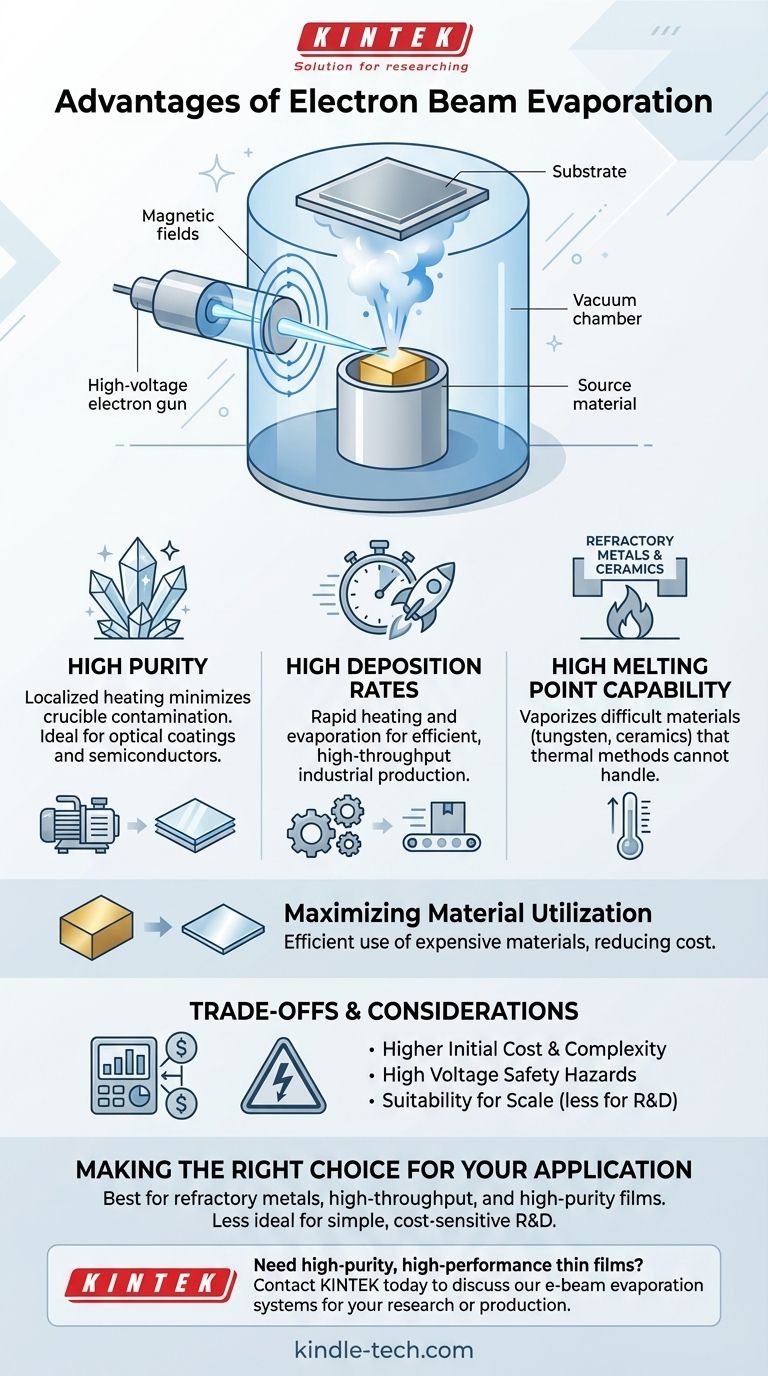
An electron beam is generated and accelerated by a high-voltage electric field, often up to 10 kV. This beam is then magnetically guided to strike a source material held in a water-cooled crucible. The kinetic energy of the electrons is converted into thermal energy upon impact, causing the material to evaporate or sublimate.
Unlocking High-Melting-Point Materials
This direct energy transfer allows the source material to reach extremely high temperatures. Unlike traditional thermal evaporation, which is limited by the melting point of the heating element (like a tungsten boat), e-beam can vaporize refractory metals and ceramics that would otherwise be impossible to process.
Achieving High Deposition Rates
The high power density of the electron beam leads to very rapid heating and evaporation. This translates directly into high deposition rates, a critical advantage for industrial applications in aerospace, tool manufacturing, and optics where throughput is essential.
Key Benefits for Film Quality and Efficiency
Beyond raw power, the precision of the electron beam process delivers significant gains in film quality and cost-effectiveness.
Ensuring High Purity
Because the electron beam heats only a small spot on the source material, the surrounding crucible remains cool. This localized heating prevents the crucible itself from outgassing or melting, drastically reducing the risk of impurities being incorporated into the deposited film. The high-vacuum environment further ensures a clean path from the source to the substrate.
Maximizing Material Utilization
The process is highly efficient. Since only the target material is vaporized, very little is wasted. This high material utilization makes e-beam evaporation a cost-effective choice, particularly when working with expensive materials common in semiconductor and optical applications.
Process Control and Repeatability
The power and position of the electron beam are precisely controllable. This allows for stable and repeatable deposition rates, which are crucial for manufacturing complex multi-layer structures like optical coatings for laser optics, architectural glass, and solar panels.
Understanding the Trade-offs
While powerful, electron beam evaporation is not the universal solution for all deposition needs. Its advantages come with specific challenges and costs that must be considered.
Higher Initial Cost and Complexity
The equipment required for e-beam evaporation is significantly more complex and expensive than that for basic thermal evaporation. The system involves a high-voltage power supply, magnetic beam-steering components, and a sophisticated water-cooling system, representing a major capital investment.
High Voltage Safety Hazards
Operating with high-voltage power sources introduces inherent safety risks. Proper training, shielding, and safety protocols are mandatory to mitigate the potential for electrical hazards during operation and maintenance.
Suitability for Scale
While excellent for industrial batch processes like ophthalmic coatings, linearly scaling the process can be difficult. This complexity can sometimes make it less suitable for certain rapid-prototyping or small-scale lab applications where simpler methods might suffice.
Making the Right Choice for Your Application
Selecting electron beam evaporation depends entirely on your material requirements, production scale, and quality standards.
- If your primary focus is depositing refractory metals or ceramics: E-beam is often the only viable PVD choice due to its ability to reach the necessary temperatures.
- If your primary focus is high-throughput industrial production: The high deposition rates of e-beam evaporation make it ideal for efficient, large-scale manufacturing.
- If your primary focus is creating high-purity optical or electronic films: E-beam's localized heating minimizes contamination, resulting in superior film quality for demanding applications.
- If your primary focus is cost-sensitive R&D with common metals: Simpler and less expensive methods, like resistive thermal evaporation, might be a more practical starting point.
Ultimately, electron beam evaporation is the expert's choice when material requirements for temperature, purity, or deposition speed exceed the capabilities of simpler thermal methods.
Summary Table:
| Advantage | Key Benefit | Ideal For |
|---|---|---|
| High Deposition Rate | Rapid vaporization for efficient production | Industrial coating, high-throughput manufacturing |
| High Material Purity | Localized heating minimizes crucible contamination | Optical coatings, semiconductor devices |
| High Melting Point Capability | Vaporizes refractory metals and ceramics | Aerospace, tooling, advanced ceramics |
| High Material Utilization | Efficient use of source material, reducing waste | Cost-effective use of expensive materials |
Need to deposit high-purity, high-performance thin films?
Electron beam evaporation from KINTEK delivers the exceptional purity, high deposition rates, and material versatility required for demanding applications in optics, semiconductors, and aerospace. Our expertise in lab equipment ensures you get the right solution for processing refractory metals and ceramics efficiently.
Contact KINTALK today to discuss how our e-beam evaporation systems can advance your research or production.
Visual Guide
Related Products
- Electron Beam Evaporation Coating Tungsten Crucible and Molybdenum Crucible for High Temperature Applications
- Electron Beam Evaporation Coating Oxygen-Free Copper Crucible and Evaporation Boat
- Electron Beam Evaporation Coating Gold Plating Tungsten Molybdenum Crucible for Evaporation
- Electron Beam Evaporation Coating Conductive Boron Nitride Crucible BN Crucible
- E Beam Crucibles Electron Gun Beam Crucible for Evaporation
People Also Ask
- What materials are used in electron beam evaporation? Master High-Purity Thin Film Deposition
- What is e-beam evaporation used for? Precision Coating for Optics, Aerospace & Electronics
- What is e-beam evaporation? Achieve High-Purity Thin Film Deposition for Your Lab
- What is the temperature of e-beam evaporation? Mastering the Two-Zone Thermal Process for Precision Films
- What is the process of e-beam coating? Achieve High-Purity, Precise Thin Films for Your Lab


