The primary advantages of ion beam deposition (IBD) are the exceptional quality of the resulting thin film and the unparalleled degree of control over the deposition process. This technique allows for the creation of films that are denser, purer, and have superior adhesion compared to other methods, all while giving the operator independent command over critical parameters like film thickness and composition.
Ion beam deposition's core strength lies in its fundamental design: it decouples the ion source from the target material. This separation gives you independent control over ion energy and flux, which is the key to unlocking precise process control and achieving superior film characteristics that other PVD methods struggle to match.
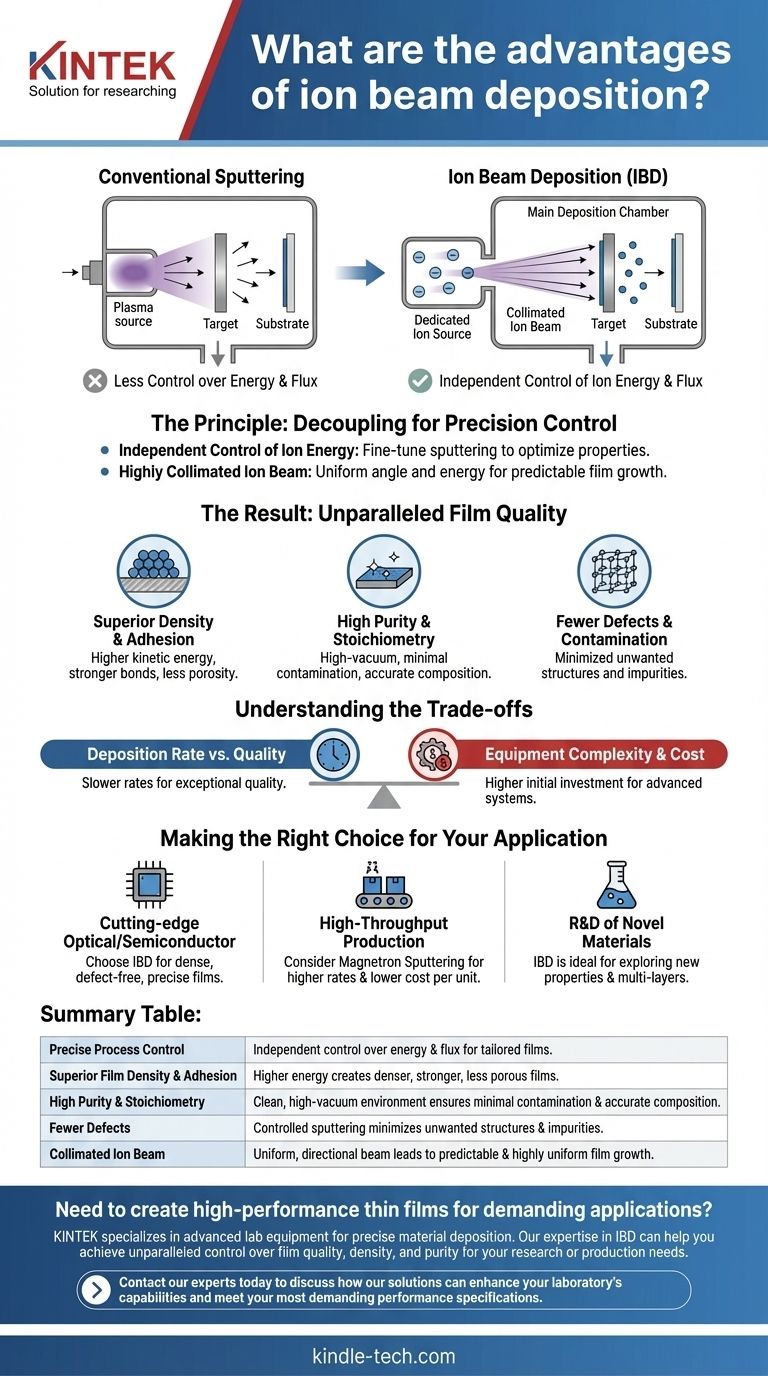
The Principle: Decoupling for Precision Control
Unlike conventional sputtering where a plasma is generated in the main chamber, ion beam deposition uses a dedicated ion source that is physically separate from the target and substrate. This is the source of its power.
Independent Control of Ion Energy
By using a separate source, the energy of the ions striking the target can be precisely controlled, independent of the number of ions (the ion flux).
This allows you to fine-tune the sputtering process to optimize the properties of the deposited material for your specific application.
Highly Collimated Ion Beam
The ions are extracted from the source and accelerated into a highly directional, or collimated, beam.
This ensures that the ions strike the target at a uniform angle and energy, leading to predictable sputtering and highly uniform film growth on the substrate.
The Result: Unparalleled Film Quality
The precise control inherent in IBD directly translates into thin films with a range of desirable properties that are critical for high-performance applications.
Superior Density and Adhesion
The sputtered atoms arrive at the substrate with higher kinetic energy compared to atoms in thermal evaporation or standard sputtering processes.
This higher energy promotes "energy bonding," creating a denser, less porous film structure with significantly stronger adhesion to the substrate surface.
High Purity and Stoichiometry
The process occurs in a high-vacuum environment, and since the plasma is confined to the ion source, contamination of the growing film from process gases is minimized.
This clean environment, combined with controlled sputtering, ensures the deposited film faithfully reproduces the composition (stoichiometry) of the target material, which is critical for complex compounds.
Fewer Defects and Contamination
The independent control over deposition parameters minimizes the growth of unwanted structures or insulating layers on the target. This leads to a more stable process and a final film with fewer defects and impurities.
Understanding the Trade-offs
No technique is without its compromises. True expertise means understanding the limitations as well as the benefits.
Deposition Rate vs. Quality
The high level of precision and control in IBD often comes at the cost of deposition speed.
While IBD produces exceptional films, its deposition rates are typically lower than those of techniques like magnetron sputtering. It prioritizes quality over quantity.
Equipment Complexity and Cost
Ion beam systems, with their dedicated high-performance ion sources and sophisticated control systems, are generally more complex and carry a higher initial capital cost than simpler PVD setups.
Making the Right Choice for Your Application
Selecting the correct deposition method depends entirely on your project's primary objective.
- If your primary focus is cutting-edge optical coatings or semiconductor devices: Choose ion beam deposition for its ability to produce dense, stable, and defect-free films with precise control over refractive index and thickness.
- If your primary focus is high-throughput production or coating large areas cheaply: Consider a technique like magnetron sputtering, which offers much higher deposition rates at a lower cost per unit.
- If your primary focus is research and development of novel materials: The flexibility and parameter control of IBD make it an ideal tool for exploring new material properties and creating complex, multi-layer structures.
Ultimately, choosing ion beam deposition is an investment in control and quality, ensuring your final product meets the most demanding performance specifications.
Summary Table:
| Advantage | Key Benefit |
|---|---|
| Precise Process Control | Independent control over ion energy and flux for tailored film properties. |
| Superior Film Density & Adhesion | Higher energy bonding creates denser, stronger films with less porosity. |
| High Purity & Stoichiometry | Clean, high-vacuum environment ensures minimal contamination and accurate composition. |
| Fewer Defects | Controlled sputtering minimizes unwanted structures and impurities in the final film. |
| Collimated Ion Beam | Uniform, directional beam leads to predictable and highly uniform film growth. |
Need to create high-performance thin films for demanding applications?
KINTEK specializes in providing advanced lab equipment and consumables for precise material deposition. Our expertise in technologies like ion beam deposition can help you achieve unparalleled control over film quality, density, and purity for your research or production needs.
Contact our experts today to discuss how our solutions can enhance your laboratory's capabilities and meet your most demanding performance specifications.
Visual Guide
Related Products
- Chemical Vapor Deposition CVD Equipment System Chamber Slide PECVD Tube Furnace with Liquid Gasifier PECVD Machine
- HFCVD Machine System Equipment for Drawing Die Nano-Diamond Coating
- Electron Beam Evaporation Coating Oxygen-Free Copper Crucible and Evaporation Boat
- RF PECVD System Radio Frequency Plasma-Enhanced Chemical Vapor Deposition RF PECVD
- Customer Made Versatile CVD Tube Furnace Chemical Vapor Deposition Chamber System Equipment
People Also Ask
- What types of substrates are used in CVD to facilitate graphene films? Optimize Graphene Growth with the Right Catalyst
- How are carbon nanotubes grown? Master Scalable Production with Chemical Vapor Deposition
- What is plasma enhanced chemical vapor deposition PECVD equipment? A Guide to Low-Temperature Thin Film Deposition
- Why is Chemical Vapor Deposition (CVD) equipment uniquely suited for constructing hierarchical superhydrophobic structures?
- What happens during deposition chemistry? Building Thin Films from Gaseous Precursors


