In short, Silicon Carbide (SiC) devices enable power electronics systems to be significantly more efficient, smaller, and lighter than those built with traditional silicon (Si). They achieve this by operating at much higher voltages, frequencies, and temperatures, fundamentally changing the design equation for applications like electric vehicles, renewable energy, and advanced industrial power supplies.
The core advantage of SiC is its wide bandgap, a fundamental material property that is roughly three times greater than silicon's. This single characteristic is the source of its ability to handle higher voltages and temperatures, which in turn allows for a revolutionary increase in power density and system efficiency.

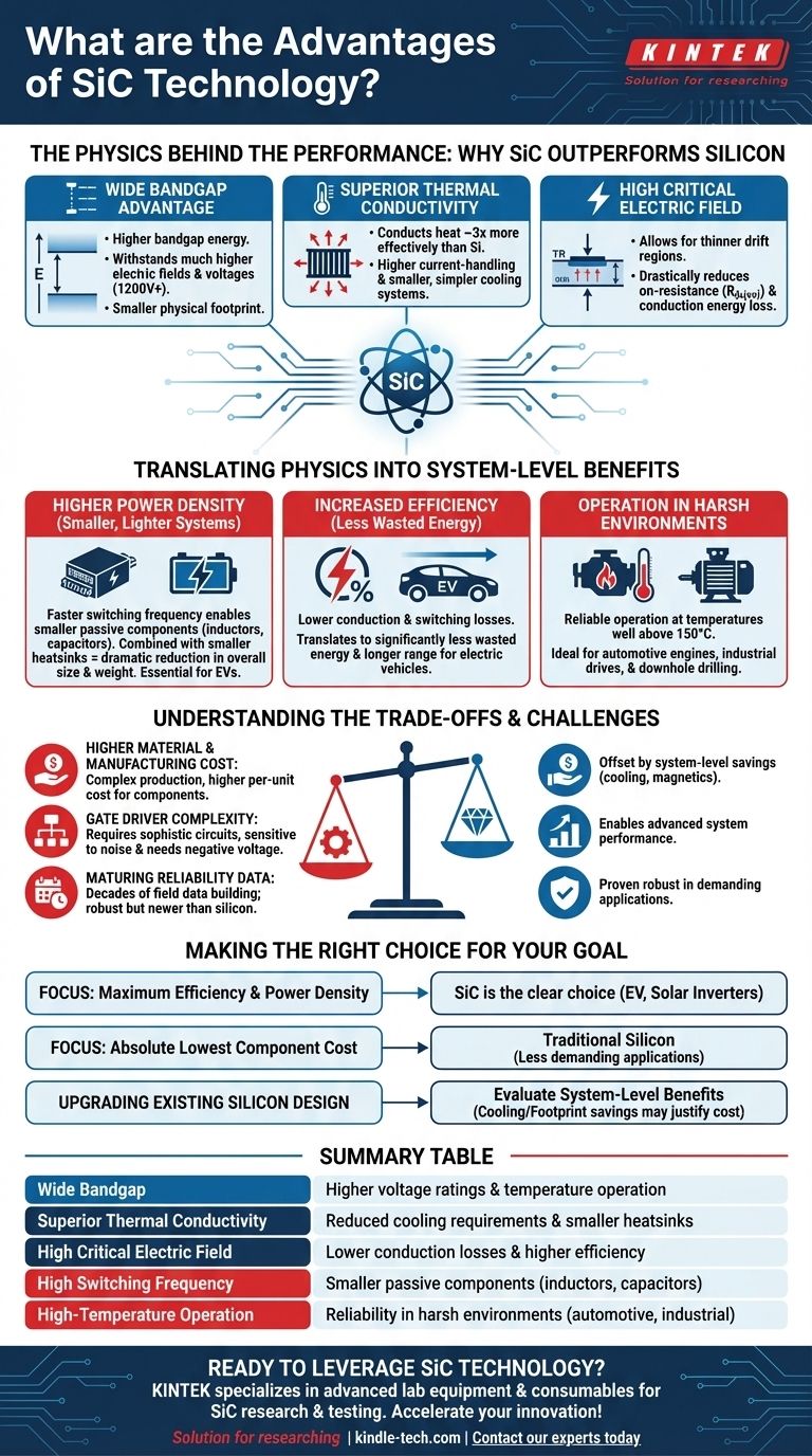
The Physics Behind the Performance: Why SiC Outperforms Silicon
To understand the system-level benefits of SiC, we must first look at its three key material advantages over silicon. These properties work together to create a superior power-switching device.
The Wide Bandgap Advantage
The bandgap is the energy required to excite an electron into a conductive state. SiC's wide bandgap allows it to withstand much higher electric fields before breaking down.
This directly enables the creation of devices with significantly higher voltage ratings (e.g., 1200V, 1700V, and beyond) in a smaller physical footprint.
Superior Thermal Conductivity
SiC is exceptionally good at conducting heat, dissipating it about three times more effectively than silicon.
This means heat is drawn away from the active part of the semiconductor die much more quickly. The practical result is higher current-handling capability and the ability to use smaller, simpler, and less expensive cooling systems (heatsinks).
High Critical Electric Field
SiC's ability to withstand a much stronger electric field (about 10x that of silicon) is a critical enabler for efficiency.
This property allows for the design of thinner, more lightly doped "drift regions" in the transistor. A thinner drift region directly translates to lower on-resistance (Rds(on)), which drastically reduces energy lost as heat during conduction.
Translating Physics into System-Level Benefits
These material properties are not just academic. They create tangible, game-changing advantages at the system level.
Higher Power Density (Smaller, Lighter Systems)
SiC devices can switch on and off much faster than silicon IGBTs. This high switching frequency allows engineers to use significantly smaller (and lighter) passive components like inductors and capacitors.
When combined with the need for smaller heatsinks, the result is a dramatic reduction in the overall size, weight, and volume of the power converter. This is a crucial advantage in space-constrained applications like electric vehicles.
Increased Efficiency (Less Wasted Energy)
Efficiency gains in SiC come from two primary sources: lower conduction losses and lower switching losses.
The low on-resistance reduces the energy lost when the device is on, while the fast switching speed reduces the energy lost during the on/off transitions. For an EV, this means less energy is wasted, translating directly to longer range from the same battery.
Operation in Harsh Environments
The combination of a wide bandgap and excellent thermal conductivity allows SiC devices to operate reliably at junction temperatures well above the 150°C-175°C limit of silicon.
This makes SiC the ideal choice for demanding applications in automotive engine compartments, industrial motor drives, and downhole drilling equipment where high ambient temperatures are common.
Understanding the Trade-offs and Challenges
While powerful, SiC is not a universal replacement for silicon. Adopting the technology requires acknowledging its specific challenges.
Higher Material and Manufacturing Cost
Producing high-quality SiC crystal wafers is a more complex and expensive process than producing silicon wafers. This results in a higher per-unit cost for SiC MOSFETs and diodes compared to their silicon counterparts.
However, this higher component cost can often be offset by system-level savings in cooling, passive components, and overall size.
Gate Driver Complexity
SiC MOSFETs require more sophisticated gate driver circuits than silicon IGBTs or MOSFETs. They are sensitive to noise and often require a negative voltage to ensure they remain reliably off.
Engineers must pay careful attention to the gate driver design and layout to prevent unintended turn-on, which can lead to device failure.
Maturing Reliability Data
Silicon has been the workhorse of the electronics industry for over 50 years, and its long-term reliability is exceptionally well-documented.
SiC is a much newer technology. While it has proven to be robust in demanding applications, the industry is still building the decades-long field data that exists for silicon.
Making the Right Choice for Your Goal
The decision to use SiC depends entirely on your system's primary performance targets.
- If your primary focus is maximum efficiency and power density: SiC is the clear choice for high-voltage applications like EV traction inverters, onboard chargers, and grid-tied solar inverters.
- If your primary focus is the absolute lowest component cost: Traditional silicon IGBTs or MOSFETs often remain the more economical solution for less demanding, lower-frequency applications.
- If you are upgrading an existing silicon-based design: Carefully evaluate the system-level benefits, as SiC's higher component cost is frequently justified by major savings on cooling, magnetics, and overall footprint.
Ultimately, SiC technology empowers you to build smaller, faster, and more efficient power systems that were previously unachievable with silicon.
Summary Table:
| Key Advantage | Impact on System Design |
|---|---|
| Wide Bandgap | Higher voltage ratings & temperature operation |
| Superior Thermal Conductivity | Reduced cooling requirements & smaller heatsinks |
| High Critical Electric Field | Lower conduction losses & higher efficiency |
| High Switching Frequency | Smaller passive components (inductors, capacitors) |
| High-Temperature Operation | Reliability in harsh environments (e.g., automotive, industrial) |
Ready to leverage SiC technology for your next power electronics project? KINTEK specializes in providing advanced lab equipment and consumables to support research, development, and testing of cutting-edge semiconductor technologies like SiC. Whether you're prototyping EV powertrains, optimizing renewable energy systems, or pushing the limits of industrial power supplies, our solutions help you achieve higher efficiency and power density. Contact our experts today to discuss how we can accelerate your innovation!
Visual Guide
Related Products
- Silicon Carbide (SIC) Ceramic Sheet Wear-Resistant Engineering Advanced Fine Ceramics
- Silicon Carbide (SIC) Ceramic Sheet Flat Corrugated Heat Sink for Engineering Advanced Fine Ceramics
- Silicon Carbide (SIC) Ceramic Plate for Engineering Advanced Fine Ceramics
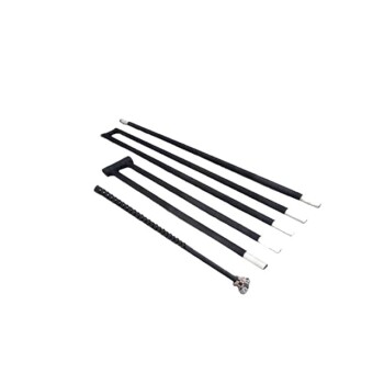
- Silicon Carbide SiC Thermal Heating Elements for Electric Furnace
- Infrared High Resistance Single Crystal Silicon Lens
People Also Ask
- What are the properties and applications of silicon carbide ceramics? Solve Extreme Engineering Challenges
- What is the type of silicon carbide? A Guide to Polymorphs, Grades, and Applications
- What is the temperature resistance of silicon carbide? Withstands Extreme Heat Up to 1500°C
- What is the strongest ceramics? Silicon Carbide Leads in Hardness & Thermal Strength
- What is the process of making silicon carbide? From Raw Materials to Advanced Ceramics