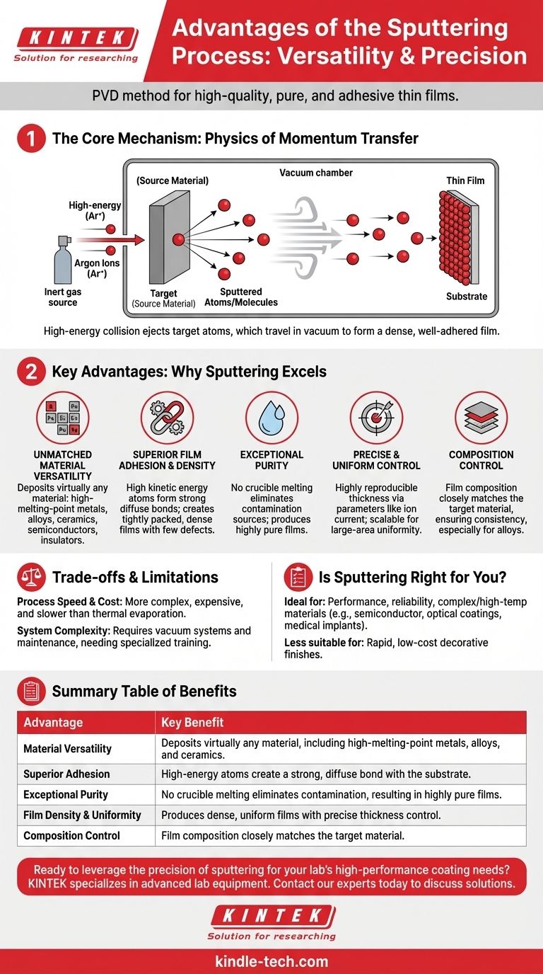
The primary advantages of sputtering are its versatility and precision. It is a physical vapor deposition (PVD) method that can deposit thin films of virtually any material—including metals, ceramics, and complex compounds—onto a substrate. This process produces coatings that are exceptionally pure, dense, and uniform, with superior adhesion compared to many other techniques.
Sputtering is not necessarily the fastest or cheapest deposition method, but it is often the superior choice when the quality, purity, and adhesion of the thin film are the most critical factors. The core advantage stems from its physical mechanism, which produces films with excellent material properties and reliability.
Why Sputtering Excels: The Core Mechanism
To understand the advantages of sputtering, it's essential to understand how it works. Unlike thermal evaporation, which boils a material, sputtering is a mechanical process on an atomic scale.
The Physics of Momentum Transfer
Sputtering uses energetic ions (typically from an inert gas like Argon) to bombard a source material, known as the target.
This collision physically knocks atoms or molecules off the target's surface. This momentum transfer process is the foundation of sputtering's key benefits.
The Role of High-Energy Atoms
The ejected atoms travel through a vacuum chamber and land on the substrate with significantly higher kinetic energy than evaporated atoms.
This high energy promotes better surface mobility, leading to denser film growth and stronger bonds with the substrate.
The Controlled Vacuum Environment
The entire process occurs in a vacuum chamber, which serves two purposes. It prevents contamination from atmospheric gases and allows the sputtered particles to travel freely from the target to the substrate.
Key Advantages in Detail
The unique mechanism of sputtering translates into several distinct and powerful advantages for producing high-quality thin films.
Unmatched Material Versatility
Because sputtering physically ejects atoms rather than melting the source, it can be used on nearly any substance.
This includes elements and compounds with extremely high melting points, alloys, semiconductors, and insulators, which are difficult or impossible to deposit using thermal evaporation.
Superior Film Adhesion and Density
The high energy of sputtered atoms helps them form a strong, diffuse bond with the substrate surface, resulting in excellent adhesion.
This energy also ensures the atoms pack together tightly, creating highly dense films with fewer pinholes or structural defects.
Exceptional Purity and Composition Control
Sputtering does not require melting the source material in a crucible, which eliminates a major source of contamination found in other methods.
Furthermore, when depositing alloys or compounds, the composition of the sputtered film is often very close to the composition of the target, ensuring consistency.
Precise and Uniform Control
Film thickness is directly related to controllable parameters like the ion current and deposition time. This allows for highly reproducible and precise thickness control.
Sputtering systems can also be designed to deposit films of uniform thickness over very large areas, making the process highly scalable for industrial production.
Understanding the Trade-offs and Limitations
No process is perfect. To make an informed decision, it's crucial to weigh the advantages of sputtering against its inherent limitations.
Process Speed and Cost
Sputtering is generally more complex and expensive than techniques like thermal evaporation. The requirement for vacuum systems, power supplies, and high-purity gas increases both the initial and operational costs.
Deposition rates for sputtering can also be lower than for some high-rate evaporation processes, making it a more time-consuming method for very thick films.
System Complexity and Maintenance
Vacuum systems require regular maintenance to perform reliably. Achieving the pristine vacuum conditions necessary for high-quality films depends on the health and cleanliness of the deposition chamber.
This complexity means that operators often require more specialized training to manage the process parameters effectively.
Is Sputtering the Right Choice for Your Application?
Choosing a deposition technique requires aligning the process capabilities with your primary goal. Sputtering's strengths make it the ideal choice for demanding applications.
- If your primary focus is performance and reliability: Sputtering is the clear choice for applications like semiconductor manufacturing, optical coatings, and medical implants where film purity, density, and adhesion are critical.
- If your primary focus is depositing complex or high-temperature materials: Sputtering's ability to handle virtually any material, including alloys and ceramics, makes it uniquely suitable for advanced material science and R&D.
- If your primary focus is rapid, low-cost coating: For applications like decorative finishes on consumer products, simpler methods like electroplating or thermal evaporation may be more cost-effective.
By understanding these core principles, you can confidently determine if sputtering's precision and quality align with your project's most critical requirements.
Summary Table:
| Advantage | Key Benefit |
|---|---|
| Material Versatility | Deposits virtually any material, including high-melting-point metals, alloys, and ceramics. |
| Superior Adhesion | High-energy atoms create a strong, diffuse bond with the substrate for exceptional film adhesion. |
| Exceptional Purity | No crucible melting eliminates contamination, resulting in highly pure films. |
| Film Density & Uniformity | Produces dense, uniform films with precise thickness control and fewer defects. |
| Composition Control | Film composition closely matches the target material, ensuring consistency. |
Ready to leverage the precision of sputtering for your lab's high-performance coating needs?
KINTEK specializes in providing advanced lab equipment and consumables for demanding applications. Our expertise in sputtering technology can help you achieve the superior film quality, purity, and adhesion your research or production requires.
Contact our experts today to discuss how our solutions can enhance your thin film processes and deliver reliable results.
Visual Guide
Related Products
- Lab Sterile Slapping Type Homogenizer for Tissue Mashing and Dispersing
- Spark Plasma Sintering Furnace SPS Furnace
- Single Punch Manual Tablet Press Machine TDP Tablet Punching Machine
People Also Ask
- Why is it necessary to use an ultrasonic cell disruptor before yeast flow cytometry? Ensure Data Accuracy
- What role does a laboratory homogenizer play in radioactive cesium detection? Ensure Accuracy in Wildlife Sampling
- What is the role of an ultrasonic cleaner during magnesium alloy coating? Ensure Superior Adhesion and Surface Purity
- What is the primary function of an ultrasonic cleaner in coating? Achieve Unmatched Substrate Purity for PVD Adhesion
- How does a homogenizer affect the quality of electrode slurry? Master Battery Consistency with High-Shear Mixing


