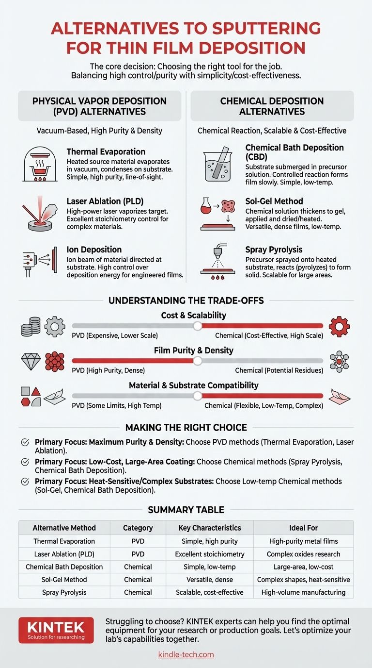
When depositing a thin film, sputtering is just one of many available techniques. The primary alternatives fall into two major families: other Physical Vapor Deposition (PVD) methods, which physically transfer material in a vacuum, and Chemical Deposition methods, which use chemical reactions to form a film on a substrate. PVD alternatives include thermal evaporation and laser ablation, while common chemical methods include chemical bath deposition, the sol-gel process, and spray pyrolysis.
The core decision is not about finding a "better" method than sputtering, but about choosing the right tool for the job. The choice involves a fundamental trade-off between the high control and purity of vacuum-based physical methods and the simplicity, cost-effectiveness, and scalability of chemical methods.
Understanding the Landscape: Physical vs. Chemical
To select a suitable alternative, it's crucial to understand the two main categories of thin film deposition. This framework clarifies the strengths and weaknesses of each approach.
Physical Vapor Deposition (PVD)
PVD processes take place in a vacuum chamber. A solid source material, or "target," is converted into a vapor, which then travels and condenses onto the substrate to form the thin film. Sputtering is a PVD method, as are its primary alternatives.
Chemical Deposition
Chemical deposition methods rely on a chemical reaction to create the film. A precursor chemical, often in a liquid solution, is applied to the substrate, and a reaction (triggered by heat, immersion, or other means) leaves behind the desired solid film. These processes often do not require a vacuum.
Physical Vapor Deposition (PVD) Alternatives
If your goal requires the high purity and density characteristic of sputtering, these PVD alternatives are your closest options. They all operate within a vacuum but use different mechanisms to vaporize the source material.
Thermal Evaporation
In thermal evaporation, the source material is heated in a vacuum until it evaporates. The resulting vapor rises, travels in a straight line, and condenses on the cooler substrate. It is simpler than sputtering but generally offers less control over the film's structure.
Laser Ablation
Also known as Pulsed Laser Deposition (PLD), this method uses a high-power laser to vaporize a small spot on the target material. The vaporized plume of material then deposits onto the substrate. PLD is excellent for depositing complex materials while preserving their chemical composition (stoichiometry).
Ion Deposition
This technique involves creating a beam of ions of the desired material and directing it toward the substrate. It offers high control over the deposition energy, which can be used to engineer the film's properties.
Chemical Deposition Alternatives
If cost, simplicity, or the ability to coat large or complex surfaces are your priorities, chemical methods offer a compelling alternative to vacuum-based PVD.
Chemical Bath Deposition (CBD)
CBD is an exceptionally simple process. A substrate is submerged in a chemical solution containing precursors. Over time, a controlled chemical reaction causes the desired film to slowly form and adhere to the substrate's surface.
The Sol-Gel Method
The sol-gel method is a "bottom-up" technique. It begins with a chemical solution (the "sol") that thickens into a gel-like state. This gel is applied to the substrate and then dried with heat or other methods, leaving a solid, dense film.
Spray Pyrolysis
This method involves spraying a precursor solution through a nozzle onto a heated substrate. The heat causes the solvent to evaporate and the precursors to react, or "pyrolyze," forming a solid film directly on the surface. It is easily scalable for large-area coatings.
Understanding the Trade-offs
No single method is universally superior. Your choice depends on a careful balance of cost, desired film quality, and the specific materials involved.
Cost and Scalability
PVD methods like sputtering and evaporation require expensive high-vacuum equipment. Chemical methods like spray pyrolysis and CBD are often far less expensive to set up and can be more easily scaled for high-volume manufacturing.
Film Purity and Density
The vacuum environment of PVD is a major advantage for creating very pure, dense films with minimal contamination. Chemical methods can sometimes leave behind residual solvents or byproducts from the reaction, potentially affecting film quality.
Material and Substrate Compatibility
Some materials are difficult to sputter effectively. Reactive sputtering can deposit insulators, but chemical methods may offer a simpler path. Furthermore, low-temperature processes like CBD or sol-gel are ideal for coating heat-sensitive substrates like plastics, which would be damaged by the high temperatures of other methods.
Making the Right Choice for Your Application
Use your primary objective to guide your decision-making process.
- If your primary focus is maximum film purity and density: PVD methods like thermal evaporation or laser ablation are strong alternatives to sputtering, offering high control in a vacuum environment.
- If your primary focus is low-cost, large-area coating: Chemical deposition methods like spray pyrolysis or chemical bath deposition offer excellent scalability and lower equipment costs.
- If your primary focus is depositing on heat-sensitive or complex-shaped substrates: Low-temperature processes like the sol-gel method or chemical bath deposition provide significant flexibility.
By aligning the unique strengths of each deposition technique with your project's specific goals, you can select the most effective and efficient path to success.
Summary Table:
| Alternative Method | Category | Key Characteristics | Ideal For |
|---|---|---|---|
| Thermal Evaporation | PVD | Simple, high purity, line-of-sight deposition | High-purity metal films |
| Laser Ablation (PLD) | PVD | Excellent stoichiometry control, complex materials | Research on complex oxides |
| Chemical Bath Deposition | Chemical | Simple, low-temperature, low-cost | Large-area, low-cost coatings |
| Sol-Gel Method | Chemical | Versatile, dense films, low-temperature | Coating complex shapes, heat-sensitive substrates |
| Spray Pyrolysis | Chemical | Scalable, large-area, cost-effective | High-volume manufacturing |
Struggling to choose the right deposition method for your specific materials and application? The experts at KINTEK are here to help. We specialize in providing lab equipment and consumables, offering tailored solutions for your thin film deposition challenges. Whether you need the high purity of a PVD system or the scalability of a chemical method, we can guide you to the optimal equipment for your research or production goals.
Let's optimize your lab's capabilities together. Contact our team today for a personalized consultation!
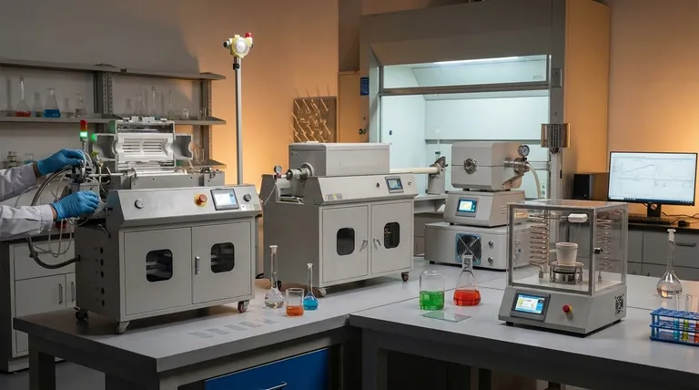
Visual Guide
Related Products
- Aluminized Ceramic Evaporation Boat for Thin Film Deposition
- Tungsten Evaporation Boat for Thin Film Deposition
- Electron Beam Evaporation Coating Oxygen-Free Copper Crucible and Evaporation Boat
- Molybdenum Tungsten Tantalum Evaporation Boat for High Temperature Applications
- Vacuum Hot Press Furnace Machine for Lamination and Heating
People Also Ask
- Why is an alumina boat selected for catalyst precursors? Ensure Sample Purity at 1000 °C
- What is the chemical method for thin film deposition? Build Films from the Molecular Level Up
- What is the source of evaporation for thin film? Choosing Between Thermal and E-Beam Methods
- Why is an alumina boat and Ti3AlC2 powder bed necessary for Ti2AlC sintering? Protect MAX Phase Purity
- Why are high-purity ceramic boats used for lignin activation? Ensure Purity & Thermal Stability


