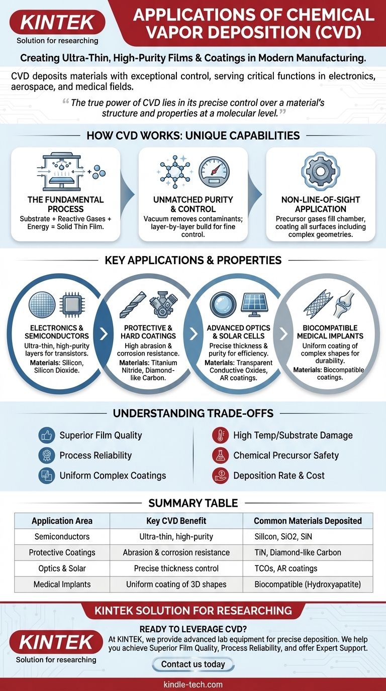
In modern manufacturing and technology, chemical vapor deposition (CVD) is a cornerstone process used to create ultra-thin, high-purity films and coatings. Its applications are driven by its unique ability to deposit materials with exceptional control, serving critical functions in industries from semiconductors and aerospace to medical devices.
The true power of CVD lies not just in its ability to apply a coating, but in its precise control over a material's structure and properties at a molecular level. This enables the creation of high-performance films that are often impossible to achieve with conventional methods.
How CVD Achieves Its Unique Capabilities
To understand the applications of CVD, we must first understand the principles that make it so versatile. The process is defined by a few key characteristics that differentiate it from other deposition techniques.
The Fundamental Process
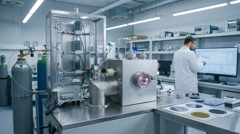
CVD involves placing a substrate (the object to be coated) inside a vacuum chamber. Reactive gases, known as precursors, are introduced, and energy (typically heat) is applied. This triggers a chemical reaction, causing a solid material to form and deposit as a thin, uniform film on the substrate's surface.
Unmatched Purity and Control
The vacuum environment is critical, as it removes contaminants that could compromise the film's purity. Because the film is built up layer by layer from a chemical reaction, operators have fine-grained control over its thickness, density, and final composition.
Non-Line-of-Sight Application
Unlike physical deposition methods that spray material in a straight line, the precursor gases in a CVD process fill the entire chamber. This allows them to coat all exposed surfaces of an object evenly, including complex shapes, internal channels, and intricate geometries.
Key Applications and the Properties That Drive Them
The unique advantages of CVD make it the go-to solution in fields where material performance is paramount. Its applications are a direct result of its core capabilities.
Electronics and Semiconductors
This is arguably the most significant application of CVD. The process is essential for building the microscopic layers of transistors and circuits on silicon wafers. Its ability to create ultra-thin, perfectly uniform, and exceptionally high-purity films is what makes modern microchips possible.
Protective and Hard Coatings
CVD is used to apply hard, durable coatings to materials like cutting tools, drill bits, and engine components. By depositing materials like titanium nitride or diamond-like carbon, it dramatically increases abrasion resistance, reduces friction, and provides protection against corrosion in high-stress environments.
Advanced Optics and Solar Cells
The precise control over film thickness and purity makes CVD ideal for optical applications. It's used to create anti-reflective coatings on lenses, specialized mirrors, and the thin, conductive layers required for high-efficiency solar panels.
Biocompatible Medical Implants
The non-line-of-sight nature of CVD allows it to uniformly coat complex medical implants, such as stents or artificial joints. These biocompatible coatings improve durability and reduce the likelihood of the body rejecting the implant.
Understanding the Trade-offs
While powerful, CVD is not the solution for every problem. Being a trusted advisor means acknowledging the limitations and circumstances where it may not be the best fit.
Substrate and Temperature Constraints
Traditional thermal CVD requires very high temperatures to initiate the chemical reaction. This can damage or warp temperature-sensitive substrates. While variants like Plasma-Enhanced CVD (PECVD) operate at lower temperatures, heat is still a primary consideration.
Chemical Precursor Management
The precursor gases used in CVD can be expensive, toxic, or highly flammable. Handling and disposing of these materials requires specialized equipment and safety protocols, adding to the operational complexity and cost.
Deposition Rate and Cost
While CVD has a commendable deposition rate for its quality, it can be slower than less precise bulk coating methods like painting or electroplating. The high cost of the equipment and materials makes it best suited for high-value applications where performance justifies the investment.
Making the Right Choice for Your Goal
Selecting the right manufacturing process depends entirely on your project's end goal.
- If your primary focus is creating ultra-pure, atomically thin layers for electronics: CVD is the industry standard due to its unmatched control over film thickness and composition.
- If your primary focus is enhancing the durability and corrosion resistance of mechanical parts: CVD provides a robust, uniform coating that strongly adheres to the surface, even in high-stress environments.
- If your primary focus is uniformly coating complex, non-flat surfaces: CVD's non-line-of-sight nature ensures that all exposed areas of the component receive an even deposition layer where other methods would fail.
Ultimately, choosing CVD is a decision to prioritize material perfection and performance over simpler, less precise alternatives.
Summary Table:
| Application Area | Key CVD Benefit | Common Materials Deposited |
|---|---|---|
| Semiconductors & Electronics | Ultra-thin, high-purity layers | Silicon, Silicon Dioxide, Silicon Nitride |
| Protective & Hard Coatings | Exceptional abrasion and corrosion resistance | Titanium Nitride, Diamond-like Carbon |
| Advanced Optics & Solar Cells | Precise control over film thickness and purity | Transparent Conductive Oxides, Anti-reflective coatings |
| Medical Implants | Uniform coating of complex 3D shapes | Biocompatible coatings (e.g., Hydroxyapatite) |
Ready to leverage CVD for your high-performance applications?
At KINTEK, we specialize in providing advanced lab equipment and consumables for precise material deposition. Whether you are developing next-generation semiconductors, durable components, or life-saving medical devices, our solutions are designed to meet the stringent demands of your laboratory.
We help you achieve:
- Superior Film Quality: Achieve the high-purity, uniform coatings essential for your research and production.
- Process Reliability: Benefit from equipment built for consistent, repeatable results.
- Expert Support: Tap into our deep knowledge of deposition technologies to optimize your workflow.
Contact us today to discuss how our CVD expertise and products can drive your innovations forward. Get in touch with our experts
Visual Guide
Related Products
- Chemical Vapor Deposition CVD Equipment System Chamber Slide PECVD Tube Furnace with Liquid Gasifier PECVD Machine
- RF PECVD System Radio Frequency Plasma-Enhanced Chemical Vapor Deposition RF PECVD
- Microwave Plasma Chemical Vapor Deposition MPCVD Machine System Reactor for Lab and Diamond Growth
- Customer Made Versatile CVD Tube Furnace Chemical Vapor Deposition Chamber System Equipment
- 915MHz MPCVD Diamond Machine Microwave Plasma Chemical Vapor Deposition System Reactor
People Also Ask
- What happens during deposition chemistry? Building Thin Films from Gaseous Precursors
- Why is Chemical Vapor Deposition (CVD) equipment uniquely suited for constructing hierarchical superhydrophobic structures?
- How are carbon nanotubes grown? Master Scalable Production with Chemical Vapor Deposition
- What is the chemical vapor deposition growth process? Build Superior Thin Films from the Atom Up
- What are the advantages of chemical vapor deposition? Achieve Superior Thin Films for Your Lab


