At its core, Chemical Vapor Deposition (CVD) is a foundational manufacturing process used to create exceptionally pure, high-performance thin films and coatings. Its applications are widespread, serving as a critical technology in the semiconductor industry for producing integrated circuits, in manufacturing for creating durable protective coatings on tools and engine parts, and in optics for developing advanced lenses and sensors.
The true value of CVD lies in its unique ability to "grow" a perfectly uniform, ultra-thin layer of material onto a surface atom by atom. This precision and its versatility in coating complex shapes make it an indispensable tool for creating the high-tech components that power our modern world.
Why CVD is a Go-To Manufacturing Process
The widespread adoption of CVD stems from a few key advantages that other deposition techniques struggle to match. These inherent properties make it the ideal choice for a range of demanding applications.
Unmatched Purity and Control
The process relies on controlled chemical reactions using high-purity precursor gases. This results in films that are exceptionally pure and dense, a non-negotiable requirement for high-performance electronics.
Furthermore, engineers have full control over the process timing and deposition parameters. This allows for the creation of ultra-thin layers with precise, repeatable thickness, down to the level of a few atoms.
Superior Conformality on Complex Shapes
CVD is a non-line-of-sight process. Unlike spray-painting, which only coats what it can directly "see," the precursor gases in a CVD chamber flow around an object, depositing a uniform film on all surfaces.
This "wrap-around" capability makes it perfect for coating components with complex geometries, ensuring even coverage inside channels, around corners, and over intricate features.
A Broad and Versatile Material Palette
Because the technique is based on chemical reactions, CVD is highly versatile and can be used to deposit a wide variety of materials. This includes semiconductors (like silicon), dielectrics (insulators), metals, and durable ceramics.
Key Industrial Applications in Detail
The unique advantages of CVD directly translate into its use in several high-value industries where performance and precision are paramount.
Semiconductor and Electronics Manufacturing
This is arguably the most significant application of CVD. The process is used at multiple stages to build the microscopic transistors and circuits found on a microchip.
Its ability to deposit ultra-thin, pure layers of conducting, insulating, and semiconducting materials is what makes modern processors and memory chips possible.
Protective and Performance Coatings
CVD is used to apply hard, wear-resistant coatings to industrial cutting tools, drills, and mechanical parts. These thin ceramic films dramatically increase durability and lifespan.
Similarly, it's used to create thermal barrier coatings on components like jet engine turbine blades, protecting them from extreme temperatures and corrosive environments.
Optics and Photonics
In the optics industry, CVD is used to apply anti-reflective coatings to lenses, improving light transmission for cameras and scientific instruments. It is also used to create specialized optical filters and waveguides.
Advanced Materials and Polymers
The process is also employed to synthesize unique materials from the ground up. This can include creating specific nanoparticles, highly pure carbon nanotubes, or polymerizing materials directly onto a surface in a vacuum environment.
Understanding the Variations of CVD
"CVD" is not a single process but a family of techniques, each optimized for different materials and applications. The primary difference is the method used to supply the energy needed to drive the chemical reaction.
Thermal CVD
This is the most fundamental form, where the substrate is heated to a high temperature, providing the thermal energy to initiate the reaction of the precursor gases on its surface.
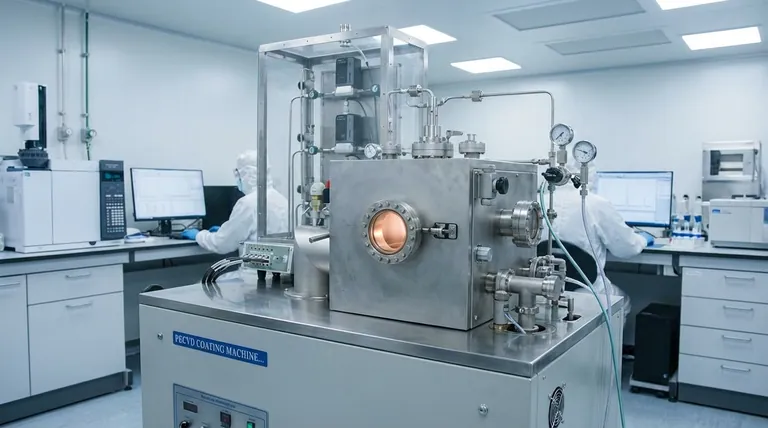
Plasma-Enhanced CVD (PECVD)
This method uses an electrically-generated plasma to energize the precursor gases instead of relying solely on high heat. This allows deposition to occur at much lower temperatures, making it suitable for coating materials that cannot withstand intense heat.
Metal-Organic CVD (MOCVD)
MOCVD uses specialized metal-organic compounds as precursors. It is a preferred method for creating very high-quality crystalline films, and is essential for manufacturing high-brightness LEDs, lasers, and certain types of solar cells.
Other Specialized Methods
Other variations exist, such as Hot-Filament CVD (HFCVD) for diamond film synthesis or Laser CVD (LCVD) for precisely depositing material in a specific, targeted area.
Making the Right Choice for Your Goal
The versatility of CVD means the specific technique is chosen based on the desired outcome.
- If your primary focus is building advanced microelectronics: Your priority is the exceptional purity, atomic-level thickness control, and material versatility offered by methods like Thermal and Metal-Organic CVD.
- If your primary focus is coating complex mechanical parts: The key advantage is the "non-line-of-sight" or conformal coverage that ensures a uniform, durable layer on all surfaces.
- If your primary focus is depositing films on heat-sensitive substrates: A lower-temperature process like Plasma-Enhanced CVD (PECVD) is the necessary choice to avoid damaging the underlying material.
Ultimately, Chemical Vapor Deposition is a cornerstone technology that enables the creation and enhancement of the most critical components in science and industry.
Summary Table:
| Application Area | Key CVD Contribution |
|---|---|
| Semiconductor Manufacturing | Deposits ultra-thin, pure layers for microchips and circuits. |
| Protective Coatings | Provides uniform, wear-resistant coatings on complex tool and engine parts. |
| Optics & Photonics | Creates anti-reflective coatings and specialized optical components. |
| Advanced Materials | Synthesizes high-purity materials like carbon nanotubes and specialized polymers. |
Ready to leverage the precision of CVD for your lab's projects?
KINTEK specializes in providing the high-quality lab equipment and consumables needed for advanced deposition processes. Whether you are developing next-generation semiconductors, durable coatings, or advanced optical materials, our expertise and products are designed to meet the stringent demands of modern laboratories.
Contact our experts today to discuss how we can support your specific application needs and help you achieve superior results.
Visual Guide

Related Products
- Chemical Vapor Deposition CVD Equipment System Chamber Slide PECVD Tube Furnace with Liquid Gasifier PECVD Machine
- RF PECVD System Radio Frequency Plasma-Enhanced Chemical Vapor Deposition RF PECVD
- Microwave Plasma Chemical Vapor Deposition MPCVD Machine System Reactor for Lab and Diamond Growth
- Customer Made Versatile CVD Tube Furnace Chemical Vapor Deposition Chamber System Equipment
- 915MHz MPCVD Diamond Machine Microwave Plasma Chemical Vapor Deposition System Reactor
People Also Ask
- What are the advantages of chemical vapor deposition? Achieve Superior Thin Films for Your Lab
- What is plasma enhanced chemical vapor deposition PECVD equipment? A Guide to Low-Temperature Thin Film Deposition
- What is the chemical vapor deposition growth process? Build Superior Thin Films from the Atom Up
- How expensive is chemical vapor deposition? Understanding the True Cost of High-Performance Coating
- What are the processes of vapor phase deposition? Understand CVD vs. PVD for Superior Thin Films


