In short, ion beam deposition (IBD) is used in applications demanding extreme precision and film quality. This includes manufacturing high-performance components like precision optics, semiconductors, specialized sensors such as gyroscopes, and durable laser coatings. It is the go-to method when the material properties of a thin film—such as its density, purity, and adhesion—are absolutely critical to the function of the final product.
The value of ion beam deposition isn't just what it creates, but how. By providing independent and precise control over deposition energy and material flux, IBD produces thin films that are denser, purer, and adhere better than those made by many other methods, making it indispensable for high-stakes applications.

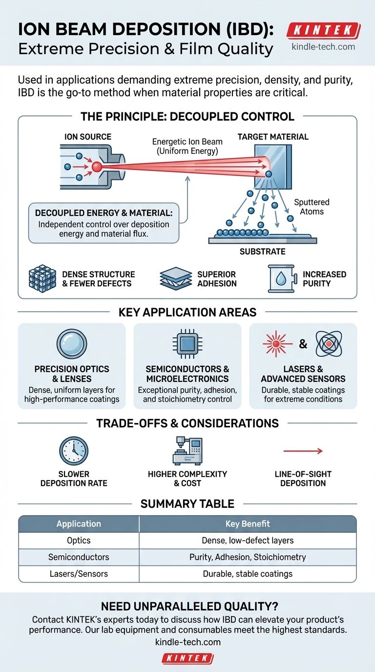
Why IBD Excels: The Principle of Control
The unique advantages of ion beam deposition stem from its fundamental architecture, which separates the creation of energetic ions from the material being deposited.
Decoupling Energy from Material
In an IBD system, a dedicated ion source generates a highly controlled, focused beam of ions with uniform energy. This beam is directed at a target material, sputtering (ejecting) atoms from it, which then travel to and coat the substrate.
This separation of the ion source and the material target is the key differentiator. It allows for independent control over the energy, angle, and flux of the depositing material, a level of precision not achievable with other common techniques.
The Result: Superior Film Properties
This granular control directly translates into higher-quality films. The energetic ions from the beam effectively "pack" the depositing atoms onto the substrate.
This leads to films with a dense structure, fewer defects, and superior adhesion to the substrate. The high-vacuum environment and focused sputtering action also result in films with increased purity.
Unmatched Stoichiometry and Thickness Control
Because the deposition process is so precisely managed, IBD provides exceptional control over the final film.
This makes it possible to maintain the ideal target composition (stoichiometry) in the deposited film and to achieve highly uniform thickness across the entire substrate, whether for microelectronics or larger optical components.
A Closer Look at Key Application Areas
The unique properties of IBD-produced films make the technology essential in several advanced industries.
Precision Optics and Lenses
Optical coatings for lenses, mirrors, and filters require dozens of layers with precisely controlled thickness and refractive index.
IBD's ability to produce extremely dense, low-defect, and uniform layers is critical for creating anti-reflection coatings and highly reflective mirrors that perform reliably and durably.
Semiconductors and Microelectronics
In semiconductor manufacturing, film purity, adhesion, and the absence of defects are non-negotiable.
IBD is used to deposit critical thin film layers where electrical or material integrity cannot be compromised. Its suitability for both small- and large-scale substrates makes it versatile for this industry.
Lasers and Advanced Sensors
High-power laser systems use specialized mirrors and coatings that must withstand intense energy without degrading. The dense, durable films created by IBD are ideal for these laser bar coatings.
Similarly, precision sensors like gyroscopes rely on components with perfectly stable and uniform material properties, a standard that IBD consistently meets.
Understanding the Trade-offs
While powerful, ion beam deposition is not the universal solution for all thin film applications. Its precision comes with clear trade-offs.
Deposition Rate
Compared to methods like magnetron sputtering or thermal evaporation, IBD is generally a slower process. This makes it less cost-effective for applications where the primary goal is to deposit a thick layer of material quickly.
System Complexity and Cost
IBD systems, with their dedicated ion sources and sophisticated control mechanisms, are more complex and carry a higher capital cost than simpler PVD equipment. The expertise required to operate and maintain them is also greater.
Line-of-Sight Deposition
Like most PVD techniques, IBD is a line-of-sight process. The material travels in a straight line from the target to the substrate. This can make it challenging to achieve uniform coatings on complex, three-dimensional objects without intricate substrate rotation and manipulation.
Making the Right Choice for Your Goal
Selecting a deposition method requires aligning the technique's strengths with your project's most critical outcome.
- If your primary focus is performance and precision: Ion beam deposition is the superior choice for creating dense, pure, and defect-free films where material properties are non-negotiable, such as in optics or semiconductors.
- If your primary focus is speed and cost for bulk coating: You should consider alternative methods like magnetron sputtering or evaporation, as IBD's lower deposition rate and higher equipment cost may not be justified.
- If your primary focus is coating complex 3D shapes: Be aware of IBD's line-of-sight nature and evaluate if the required substrate manipulation is feasible and cost-effective for your project.
Ultimately, ion beam deposition is a specialized tool leveraged when the integrity and performance of a thin film are paramount.
Summary Table:
| Application Area | Key Benefit of IBD |
|---|---|
| Precision Optics & Lenses | Dense, low-defect layers for high-performance coatings |
| Semiconductors & Microelectronics | Exceptional purity, adhesion, and stoichiometry control |
| Lasers & Advanced Sensors (e.g., Gyroscopes) | Durable, stable coatings that withstand extreme conditions |
Need a thin film with unparalleled quality?
If your project demands extreme precision, purity, and film integrity—for applications in semiconductors, optics, or advanced sensors—KINTEK's expertise in ion beam deposition is your solution. Our lab equipment and consumables are designed to meet the highest standards, ensuring your films are dense, defect-free, and perfectly adherent.
Contact our experts today to discuss how IBD can elevate your product's performance.
Visual Guide
Related Products
- Chemical Vapor Deposition CVD Equipment System Chamber Slide PECVD Tube Furnace with Liquid Gasifier PECVD Machine
- HFCVD Machine System Equipment for Drawing Die Nano-Diamond Coating
- Electron Beam Evaporation Coating Oxygen-Free Copper Crucible and Evaporation Boat
- RF PECVD System Radio Frequency Plasma-Enhanced Chemical Vapor Deposition RF PECVD
- Customer Made Versatile CVD Tube Furnace Chemical Vapor Deposition Chamber System Equipment
People Also Ask
- What are the advantages of chemical vapor deposition? Achieve Superior Thin Films for Your Lab
- How are carbon nanotubes grown? Master Scalable Production with Chemical Vapor Deposition
- What is the chemical vapor deposition growth process? Build Superior Thin Films from the Atom Up
- What types of substrates are used in CVD to facilitate graphene films? Optimize Graphene Growth with the Right Catalyst
- What are the processes of vapor phase deposition? Understand CVD vs. PVD for Superior Thin Films


