In essence, physical vapor deposition (PVD) is used to apply high-performance thin-film coatings onto a material's surface to enhance its properties. Key applications include creating dense, temperature-resistant coatings for aerospace components, depositing hard, wear-resistant layers on industrial cutting tools, and applying specialized optical and conductive films for semiconductors and solar panels.
The core value of PVD lies in its precision. It is a "line-of-sight" vacuum deposition method that physically transfers a pure material onto a substrate, making it the ideal choice for creating extremely high-performance surface layers where direct access to the surface is possible.
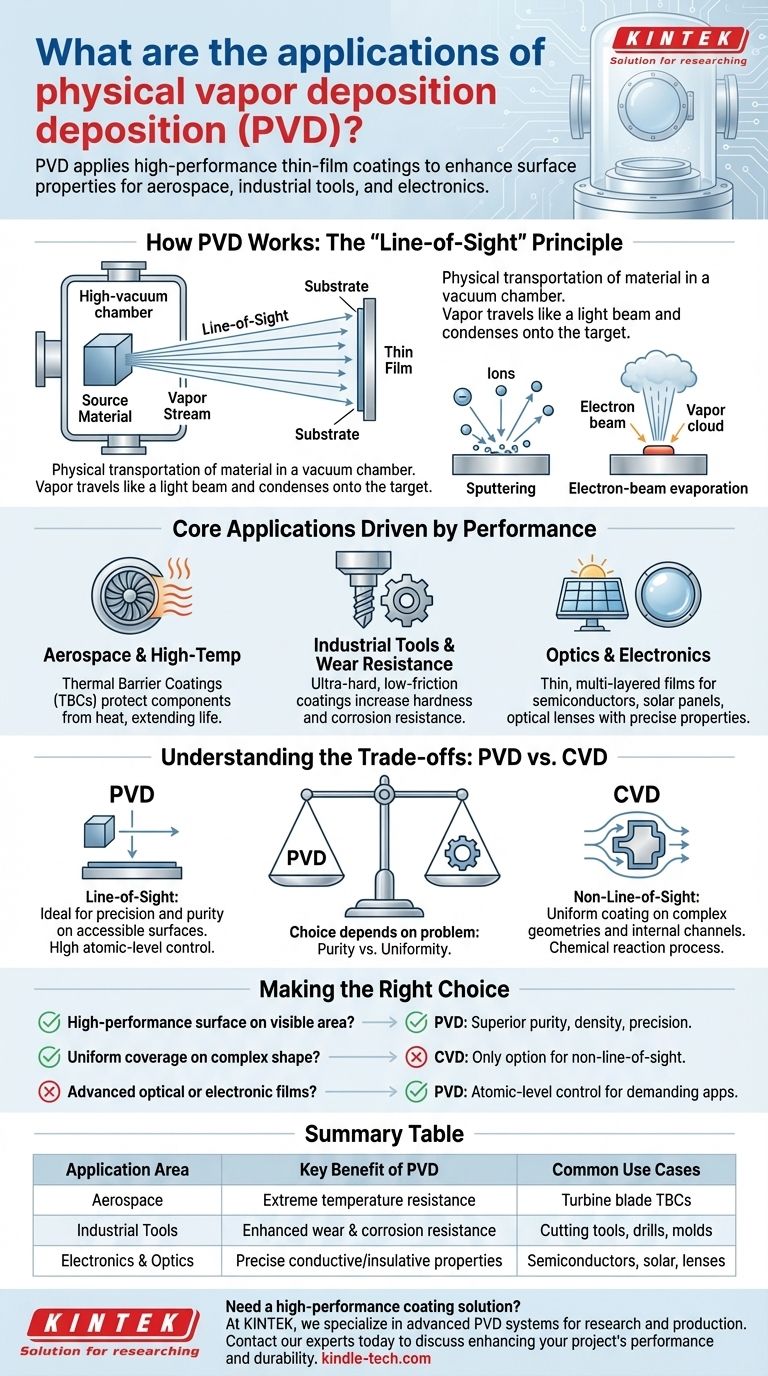
How PVD Works: The "Line-of-Sight" Principle
Physical Vapor Deposition is fundamentally a process of physical transportation. It operates within a high-vacuum chamber where a solid source material is converted into a vapor.
This vapor then travels in a straight line—like a beam of light—and condenses onto the target object, or substrate, forming a thin, dense film.
Key PVD Mechanisms
Two common methods for vaporizing the source material are sputtering and evaporation.
Sputtering involves bombarding the source material with high-energy ions, which physically knock atoms off its surface. These ejected atoms then deposit onto the substrate.
Electron-beam evaporation uses a high-energy beam of electrons to heat and vaporize the source material, creating a vapor cloud that condenses onto the part being coated.
The Defining Characteristic: Precision Control
Because the material travels in a straight line from source to substrate, PVD offers exceptionally fine control over the thickness, structure, and purity of the resulting film. This precision is critical for advanced applications in electronics and optics.
Core Applications Driven by Performance
The applications of PVD are directly tied to the functional benefits its coatings provide. It is chosen when a specific surface property—not bulk material—is the limiting factor for performance.
Aerospace and High-Temperature Environments
In the aerospace industry, components like turbine blades are subjected to extreme temperatures. PVD is used to apply thermal barrier coatings (TBCs).
These dense ceramic films act as insulators, protecting the underlying metal from heat damage and extending the component's operational life and durability.
Industrial Tools and Wear Resistance
For cutting tools, drills, and molds, the primary failure mode is wear and corrosion. PVD applies ultra-hard, low-friction coatings.
These layers, often just a few microns thick, dramatically increase hardness and corrosion resistance, allowing tools to last longer and perform better in harsh industrial environments.
Optics and Electronics
PVD is fundamental to modern electronics and optics. It is used to deposit the thin, multi-layered films required for manufacturing semiconductors, solar panels, and optical lenses.
The process's precision allows for the creation of films with specific reflective, anti-reflective, conductive, or insulating properties essential for these devices to function correctly.
Understanding the Trade-offs: PVD vs. CVD
To truly understand PVD's role, it's essential to compare it with its primary alternative: Chemical Vapor Deposition (CVD). The choice between them depends entirely on the problem you need to solve.
The "Line-of-Sight" Limitation of PVD
PVD's greatest strength—its direct, line-of-sight deposition—is also its main limitation. It cannot effectively coat complex internal geometries or the "backside" of an object that isn't directly facing the vapor source.
The Versatility of CVD for Complex Geometries
Chemical Vapor Deposition, by contrast, is a non-line-of-sight process. It uses gaseous chemical precursors that react on all heated surfaces of a substrate.
This allows CVD to create a highly uniform coating over parts with intricate shapes, holes, and internal channels, which would be impossible for PVD to cover evenly.
Purity vs. Uniformity
PVD excels at depositing exceptionally pure materials with precise control over thickness, which is ideal for optical and electronic applications.
CVD excels at creating highly uniform and conforming coatings over complex shapes, making it ideal for applications where complete, even coverage is the primary requirement.
Making the Right Choice for Your Goal
Your application's specific requirements will determine whether PVD or an alternative like CVD is the appropriate technology.
- If your primary focus is a high-performance surface on a visible area: PVD is the superior choice for its purity, density, and precision control over film properties.
- If your primary focus is uniform coverage on a complex shape: CVD is the only practical option due to its non-line-of-sight chemical reaction process.
- If your primary focus is creating advanced optical or electronic films: PVD provides the atomic-level control over thickness and composition needed for these demanding applications.
Ultimately, selecting the right deposition technology begins with a clear understanding of your component's geometry and its required surface function.
Summary Table:
| Application Area | Key Benefit of PVD Coating | Common Use Cases |
|---|---|---|
| Aerospace | Extreme temperature resistance | Turbine blade thermal barrier coatings (TBCs) |
| Industrial Tools | Enhanced wear and corrosion resistance | Cutting tools, drills, and molds |
| Electronics & Optics | Precise conductive/insulative properties | Semiconductors, solar panels, optical lenses |
Need a high-performance coating solution for your laboratory equipment?
At KINTEK, we specialize in providing advanced lab equipment and consumables, including PVD systems, to meet your specific research and production needs. Whether you are developing new semiconductor materials, creating more durable tools, or advancing aerospace components, our expertise can help you achieve superior surface properties with precision and reliability.
Contact our experts today via our Contact Form to discuss how our PVD solutions can enhance your project's performance and durability.
Visual Guide
Related Products
- Chemical Vapor Deposition CVD Equipment System Chamber Slide PECVD Tube Furnace with Liquid Gasifier PECVD Machine
- RF PECVD System Radio Frequency Plasma-Enhanced Chemical Vapor Deposition RF PECVD
- Customer Made Versatile CVD Tube Furnace Chemical Vapor Deposition Chamber System Equipment
- Microwave Plasma Chemical Vapor Deposition MPCVD Machine System Reactor for Lab and Diamond Growth
- Custom CVD Diamond Coating for Lab Applications
People Also Ask
- What are the processes of vapor phase deposition? Understand CVD vs. PVD for Superior Thin Films
- What happens during deposition chemistry? Building Thin Films from Gaseous Precursors
- How expensive is chemical vapor deposition? Understanding the True Cost of High-Performance Coating
- What is plasma enhanced chemical vapor deposition PECVD equipment? A Guide to Low-Temperature Thin Film Deposition
- What are the advantages of chemical vapor deposition? Achieve Superior Thin Films for Your Lab


